The extraordinary potential of nanoscience (from a researcher with extraordinary potential)
Yashaswi Nalawade is currently working on her PhD in Professor Jonathan Coleman’s Laboratory at Trinity College in Ireland. The team is working on the synthesis of low-dimensional nanostructures which will help usher in the next generation of nanotechnology across a range of fields
Nanotechnology is a branch of science that is concerned with working at the nanoscale, that is, materials that are around 1 to 100 nanometres. One nanometre is one billionth of a metre, which is unimaginably small – but these materials offer enormous potential for the development of a range of different technologies that could shape the world of the future. For instance, electronics is increasingly reliant on nanomaterials and the rise of 2D and 3D printing has led to a need for researchers to invent and/or develop materials that are suitable to print electronics.
To print electronics, ink is needed – but not just any ink. These inks need to be conducting, semi-conducting or insulating (which is also known as dielectric). With these requirements in mind, Yashaswi Nalawade is working at Professor Jonathan Coleman’s laboratory, which is based within Trinity College at the University of Dublin in Ireland. Yashaswi is a PhD student with a keen interest in physics and nanoscience but also motivated by the ways her work contributes to overcoming some of the problems society will face in the future.
WHY IS THERE A NEED FOR YASHASWI’S RESEARCH?
There has been a recent shift in nanoscience from the production and characterisation of 2D nanomaterials from layered crystals, to optimising and tailoring functional inks that are suitable for printing electronics. The growth in printed transistors and supercapacitors needs to be supported by a parallel growth in printed dielectrics, and Yashaswi’s investigations seek to facilitate this. “My research involves synthesising and optimising insulating inks – i.e. going from a dielectric layered crystal to 2D nanosheets of insulating nature which can then be tailored into inks to be printed,” explains Yashaswi. “The field of printed electronics, albeit very young, has shown promise in everyday applications to replace silicon-based devices. It allows for the development of wearable electronics, cheap, flexible and disposable devices which could have major societal impact and change our relationship with technology. It can also facilitate research that incorporates nanotechnology in sustainable energy and will help us make advancements in solar panels, wind turbines, etc.”
HOW IS THE LABORATORY SYNTHESISING NANOMATERIALS?
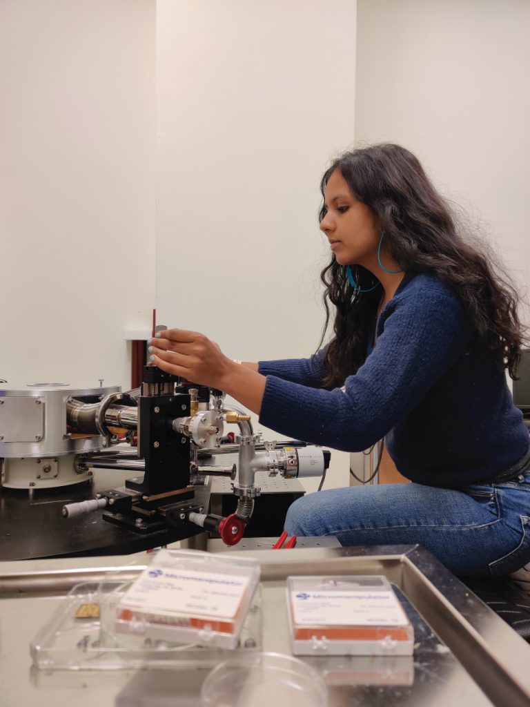
While the methods for synthesising nanomaterials are quite straightforward – they can be done with household items, such as graphite from pencils and a kitchen blender! – developing these materials into complex designs and devices is where the challenge for Yashaswi and her colleagues lies.
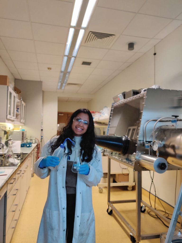
The bonding in layered crystals is such that the atoms in the same plane are bonded by strong covalent bonds, whereas the interlayer bonding is due to the weaker ‘Van der Waals’ attraction (where the interaction between atoms depends on how close together they are). This enables the team to separate the layers and produce 2D nanosheets. “We use a technique called Liquid Phase Exfoliation (LPE) to synthesise our 2D nanomaterial dispersions. Powder of the bulk crystal is mixed with a specific solvent and sonicated, i.e. subjected to ultrasound energy for several hours,” says Yashaswi. “The sonic energy creates bubbles or ‘cavitations’ within the liquid, which, on collapsing, release large amounts of shear energy that splits apart the layers in the crystal, thus producing 2D sheets in the liquid dispersion.”
The nanosheets produced by this technique are a range of sizes and thicknesses. From there, the team use a technique called Liquid Cascade Centrifugation, which involves subjecting the dispersion to centrifugation so that the centrifugal force pulls the material out of the solution. Interestingly, the size of the nanosheet extracted is dependent on the speed at which the centrifuge is run at, so the higher the speed, the smaller the nanosheets.
WHAT MATERIALS IS THE TEAM FOCUSED ON?
The team that Yashaswi is a part of is working on the synthesis of low-dimensional nanostructures, including graphene, the aforementioned dielectric inks, and boron-nitride nanotubes. Graphene is produced from graphite and was the material that gained the field of 2D nanomaterials attention around the world. Graphite is a well-known conductor of electricity, but graphene boasts even better properties, such as high electrical conductivity and high thermal conductivity. In addition, a sheet of graphene can be more than 50 times stronger than steel and as pliable as rubber!
Boron-nitride (BN) has a structure that is almost the same as graphene but is also insulating. Both graphene and BN are easily available, cheap, non-toxic and easy to handle, making them extremely suited to a range of applications.
In addition, the team works extensively with TMDs (Transition Metal Dichalcogenides) – a group of semiconducting materials which can be exfoliated to make semiconducting nanosheets, which allow the fabrication of transistors and optoelectronic devices, etc.
WHAT IS YASHASWI’S ROLE IN THE RESEARCH?
Yashaswi investigates dielectric nanomaterials and the deposition of dielectric films suitable for printed electronics. This involves the synthesis of dielectric nanosheets in dispersion and tailoring them into an ink that is suitable for printing. “Recently, I have contributed to this research by publishing a paper which details the liquid phase exfoliation of bismuth oxychloride (BiOCl) nanosheets, a high permittivity insulating material and further demonstrating BiOCl dielectric capacitors deposited using an aerosol-jet printer,” explains Yashaswi. “A stacked heterostructure was printed with graphene electrodes sandwiching an insulating film of BiOCl. The working of the capacitor was studied to characterise the quality and properties of the dielectric films.”
The publication of Yashaswi’s first paper – while she is working on her PhD – is a major encouragement for her and a sign that she is working in the right field. The feeling of satisfaction and pride when your research has been published can hardly be overstated and it really is a remarkable achievement. It will also likely be the first paper of many!
WHERE DOES YASHASWI SEE HER RESEARCH HEADING?
Given that Yashaswi has demonstrated that BiOCl is a strong candidate for dielectric films used in printed devices (i.e. it has a high dielectric constant and has been demonstrated to be suitable for printing), her research will likely usher in a move towards further characterisation of 1D and 2D dielectric materials and their composites. Further research needs to be conducted to improve specific properties of BiOCl, which may even require adding other materials to form composites that boast amazing properties. Whatever happens in the future, the fact is that printing electronic devices heavily relies on dielectric films and inks, so Yashaswi’s research will bring immense value to the field of nanotechnology and help to shape the future developments within it.
 YASHASWI NALAWADE
PhD student in the Chemical Physics of Low-Dimensional Nanostructures Group, School of Physics, Trinity College, University of Dublin, Ireland
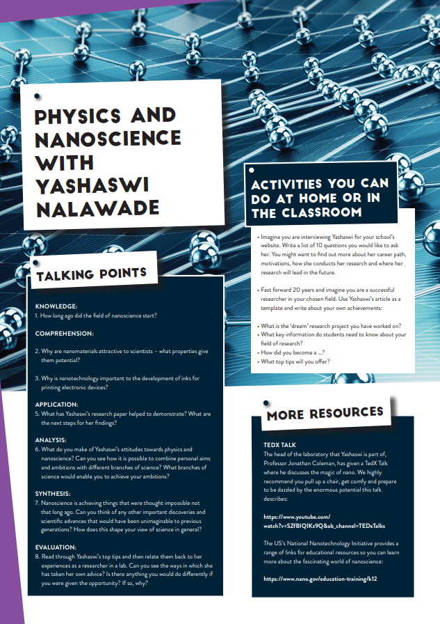
FIELD OF RESEARCH: Physics and Nanoscience
RESEARCH PROJECT: Yashaswi is working on the synthesis of low-dimensional nanostructures, including graphene, dielectric inks and boron-nitride nanotubes. The findings will facilitate research incorporating nanotechnology in a wide range of fields and applications.
FUNDER: Yashaswi’s work is supported by her supervisor, Professor Jonathan Coleman. Professor Coleman’s research group is funded by the European Research Council and Science Foundation Ireland.
Reference
https://doi.org/10.33424/FUTURUM138

When new technology and new products using sensitive materials are being designed and developed, it is essential that the environment is clean – really clean. Clean to the extent that there is not even a mote of dust flying in the air. One product that requires such an environment is semiconductor devices, which are used in a wide range of electronics, such as computer chips in laptops, personal computers and smartphones. Hence, these semiconductor devices are an essential requirement for modern life – you (and everyone you know) use them every day, even if you do not know it.
But think of how difficult it is to create a space where not even dust can get inside. It is with this aim that Professor Klara Nahrstedt, of the Computer Science Department at the University of Illinois, Urbana-Champaign, has embarked on her current project. Klara and her team from the Coordinated Science Laboratory (CSL) (graduate students Zhe Yang and Beitong Tian) and Holonyak Micro-and-Nanotechnology Laboratory (HMNTL) (graduate students Patrick Su and Robert Kaufman, principal research engineer Dr Mark McCollum, and Electrical and Computer Engineering Professor John Dallesasse) formed the project entitled Sensory Network infrastructure for Scientific Lab Environments (SENSELET). The aim is to assist scientists in maintaining environmental control within cleanroom labs to fabricate new materials and semiconductor chips.
WHY ARE CLEANROOMS SO IMPORTANT?
If a mote of dust lands on a TV screen it hardly matters; the screen is so big that a dust particle is inconsequential. However, the experimental structures of devices in cleanrooms that the SENSELET project monitors are made on the micron to nanometre scale. A nanometre is one billionth of a metre, which means that the structures of these devices are often smaller than a single dust particle and can ruin the manufacturing process of these devices – this comes at an economic cost, but it can also lead to semiconductor chip failures and significant delays in semiconductor research. Cleanrooms help prevent this from happening by constantly filtering the air throughout the room to ensure there is virtually no dust or particles.
It is not only problems with dust that Klara and her team are working to overcome. There are other environmental parameters, such as temperature and humidity, that must be strictly controlled. This is particularly important for polymers (materials made of long, repeating chains of molecules) such as photoresist, which is a light-sensitive material that is part of a crucial process in the electronics industry. If the temperature and humidity are not kept within certain parameters, they can result in the device having different dimensions from those required, causing the device to fail and, ultimately, the whole chip to fail.
HOW IS SENSELET HELPING TO ENSURE THAT CLEANROOMS ARE EFFECTIVE?
Steps can be taken to try and ensure that the cleanrooms in which specific devices are being built operate properly. However, it is necessary to continuously monitor the room’s environment to discover whether the required conditions are being maintained. Klara and her team have put their computer science knowledge to use to build SENSELET, which can collect and track data automatically, thereby ensuring researchers can monitor and predict the environmental behaviour around scientific equipment (e.g. microscopes) in any given cleanroom. Ultimately, this facilitates a proactive rather than reactive approach and enables researchers to work around the clock without fear of damaging equipment.
WHAT ARE THE MAIN COMPONENTS OF SENSELET?
SENSELET consists of three components. “The first component is the environment monitoring module, which is composed of temperature, humidity, air-flow and water leakage sensors – and a small device we call SenseEdge to collect sensory data and push data to the remote cloud called SenseCloud,” explains Klara. “The second component is the data storage engine residing in the SenseCloud. This module runs a time series database which stores all the sensory data. The third component, residing in the SenseCloud, is the visualisation and alert module, which provides visualisation dashboards to lab administrators and sends out alerts when environmental data exceed a normal range.”
Sensors are deployed in key locations within the cleanroom to monitor the environment. In addition, they sample and track the environmental information over time so that users can access an overview of the cleanroom environmental data on a periodic basis.
WHAT CHALLENGES HAS KLARA FACED DURING THE PROJECT?
The most difficult problem has been reliability, closely followed by maintenance of sensors. “We do not have the same budget as the semiconductor companies do, so we rely on off-the-shelf commercial sensors which do not have very high reliability guarantees,” says Klara. “In addition, we do not have sufficient staffing to constantly monitor and maintain the sensory hardware and the corresponding sensing services. Hence, we need to build the system as robust as possible. To address this, we designed a watchdog mechanism to manage the sensors.”
Another issue concerns the heterogeneity of sensors, that is, the fact that sensors are of different types. Klara and the team are working to ensure SENSELET supports different sensor types easily and makes it simple to add or replace sensors. The final challenge is related to time-sensitive data analysis – it is essential that SENSELET can trigger warnings at a time that is most beneficial. Klara and the team have been working to shorten the time between the occurrence of an abnormal sensory event and the alert. The aim is to create a system that can predict future abnormal events based on the current situation; the benefits to manufacturers of electronic equipment would be enormous.
WHAT HAVE BEEN THE KEY SUCCESSES OF THE PROJECT?
SENSELET has been used within the University of Illinois, Urbana-Champaign, where Klara is based, and provided quantifiable data showing that the humidity control is not within specifications. The system has also identified other environmental problems across a range of academic scientific locations within the HMNTL. “A dashboard has been created to notify users of the current temperature and humidity deviations, measured inside the cleanroom, as well as historical data being tracked every minute,” explains Klara. “This data has proved useful in helping cleanroom lab managers and researchers adjust their management and scientific processes. Overall, SENSELET also demonstrated a low-cost, high performance sensory network capable of micro-climate monitoring and being deployed in academic scientific environments, such as cleanrooms for micro-climate monitoring.”
There is still more work to be done, but SENSELET is already proving its worth – and further advances in the technology will save a tremendous amount of time, effort and money. It is fitting that Klara and her graduate students are putting their computer science expertise to use to enable the materials and semiconductor device fabrication research and development environment that will advance the field of computing!
YASHASWI NALAWADEPhD student in the Chemical Physics of Low-Dimensional Nanostructures Group, School of Physics, Trinity College, University of Dublin, Ireland
FIELD OF RESEARCH: Physics and Nanoscience
RESEARCH PROJECT: Yashaswi is working on the synthesis of low-dimensional nanostructures, including graphene, dielectric inks and boron-nitride nanotubes. The findings will facilitate research incorporating nanotechnology in a wide range of fields and applications.
FUNDER: Yashaswi’s work is supported by her supervisor, Professor Jonathan Coleman. Professor Coleman’s research group is funded by the European Research Council and Science Foundation Ireland.
ABOUT PHYSICS AND NANOSCIENCE
It is mind-blowing that scientists have found a way to work with materials that are so extraordinarily small. Manipulating and making use of materials that are smaller than the width of a human hair sounds like something from the realms of science fiction, but it is science fact! At the incredibly small scales we are talking about, materials demonstrate properties that simply do not exist on larger scales, which is exciting for a range of different fields because what was once thought impossible to achieve is now possible.
Nanomaterials have a high surface area to volume ratio, which means they can function as extremely effective catalysts and speed up chemical reactions. The possibilities within the field were thought unrealistic just a few years ago, which should tell us that the possibilities for the future are probably beyond what most of us can imagine today.
Yashaswi is just starting out in her research career, but she will be a doctor before long and has already had one of her research papers published. It appears that her career pathway is going to be very exciting and her work could help us overcome issues regarding climate change, global warming and the development of sustainable technologies (as well as many other applications).
WHAT DOES YASHASWI FIND INTERESTING ABOUT HER WORK?
Yashaswi believes that working in a lab is very rewarding because you get to build something from scratch, and getting that something working is a very satisfying feeling! In her lab, she is surrounded by other people with a keen interest in physics and nanoscience, and they can all ask each other questions and work together to design experiments to answer the questions they have. “I was sure I wanted to pursue something in applied physics that involved doing experiments and working with my hands in a lab,” says Yashaswi. “With that in mind, nanoscience was the obvious choice. It is a fast-growing field of applied physics and has much scope in commercial applications.”
WHAT ARE THE MAIN MISCONCEPTIONS THAT PEOPLE HAVE?
“People think that nanoscience is making tiny robots that would be inserted into our bodies and swim around and fix problems, but these are misleading notions,” says Yashaswi. “In reality, when we reduce the size of objects to nanoscale, they behave very differently to their ‘bulk’ version. For example, if we were to build a nanorobot to swim in your blood, it would experience a much higher viscous force from the medium – it would be like us trying to swim in oil. This would require the robot to have a motor to propel it forward. But of course, it is unrealistic to have a motor that powerful which is that small.”
WHAT WOULD BE YASHASWI’S DREAM PROJECT TO WORK ON?
Yashaswi is keen to work on something related to sustainable energy technology – and nanoscience has extraordinary potential in this area. It is worth remembering that nanoscience is still in its infancy – it only began around 12 years ago, but researchers like Yashaswi will help ensure that nanotech becomes an ever-present part of our daily lives.
EXPLORE A CAREER IN NANOSCIENCE
• Nanowerk goes into some detail about what nanotechnology is and why it is important. The site also includes a wealth of information on different nanomaterials, resources and jobs within the field.
• FutureLearn hosts introductory courses on how nanotechnologies are applied in various fields, such as healthcare. You can join many courses for free and it is conducted 100% online, so you can study from anywhere.
• As a PhD student, you receive a stipend of around £16,000 to £18,000 a year, for a period of four years.
• According to the National Careers Service, the salary for an experienced nanotechnologist varies, depending on the level of experience and the specific job title, with the upper pay scale around £40,000.
PATHWAY FROM SCHOOL TO NANOSCIENCE
• Yashaswi says that students should certainly consider studying physics, chemistry and maths in school and beyond. If there are any statistics classes or modules offered you should think about taking them, as they will prove to be a big help for budding nanoscientists.
• 2 or 3 A levels, or equivalent, including maths and a science for a degree.
• Relevant degree subjects include nanoscience, physics, chemistry, electronics engineering, materials science and computer science. You will usually need a degree or a postgraduate master’s qualification in nanotechnology, or a related course which includes nanotechnology.
https://nationalcareers.service.gov.uk/job-profiles/nanotechnologist
HOW DID YASHASWI BECOME A NANOSCIENTIST?
WHAT WERE YOUR INTERESTS AS A CHILD?
I was always only ever interested in science as a child. This was probably because I was constantly exposed to it as both my parents are from a science background too! I wouldn’t say I was a voracious reader or was watching loads of animal/nature shows, but there was always an underlying curious mind and any problem was approached scientifically.
WHO OR WHAT INSPIRED YOU TO BECOME A SCIENTIST?
I was introduced to a lot of big picture physics questions from a young age by my father – he would always tell me the problems scientists and mathematicians were working on. This instilled a curiosity in me to be involved in these topics myself.
WHAT ATTRIBUTES HAVE MADE YOU SUCCESSFUL AS A SCIENTIST?
I am naturally curious, always asking why and how until I am satisfied with the answer, always questioning why things are the way they are. Most importantly, I’m not afraid to say I don’t know or understand something. There’s no shame in that and, in fact, it helps you acquire more knowledge.
HOW DO YOU OVERCOME OBSTACLES IN YOUR WORK?
I actually work much better in a team than on my own – I am quite good at discussing a problem and troubleshooting with my group members. So, any time I encounter an obstacle, I find it helpful to discuss it with my colleagues or supervisor.
WHAT ARE YOUR PROUDEST CAREER ACHIEVEMENTS SO FAR AND WHAT ARE YOUR AMBITIONS FOR THE FUTURE?
I am generally proud I haven’t lost my interest and thirst for science – it’s definitely not easy to maintain. Getting my PhD position in a well-renowned research group was a big moment for me and a step in the right direction! Now that I am in my final year and have published a paper, I feel much more confident I’m doing what I love. As of now, I hope in the future I become involved in something that is meaningful, with a clear goal towards bettering our lives (for example, I would love to be involved in researching sustainable energy technology), without losing my love of science.
YASHASWI’S TOP TIPS
01 Keep at it! You do not have to be a genius to have a career in science – you just have to work hard and have a genuine interest in it. Never be afraid to say that you do not understand something, especially as most people around you have the same questions that you do. Ask for help as much as you can!
02 Avoid specialising in one niche topic, as a broad understanding will provide you with the skills, knowledge and experience you will need to focus on a more specific area in the future. Instead of direct entry courses, perhaps consider choosing general science courses for your first years in college.
03 Ask for internships and work experience in labs during college as much as you can. A lot of professors are looking for summer students and it is a great way to get a taste of research before making any big decisions.
Write it in the comments box below and Yashaswi will get back to you. (Remember, researchers are very busy people, so you may have to wait a few days.)