Examining the extremely small
Nanoscience is the study of the very small. It has many applications, from creating molecules that can deliver drugs to specific targets in the body, to improving the efficiency of solar cells. In Munich, Germany, nanoscientists from all fields are coming together to share ideas and expertise, thanks to the work of the Center for NanoScience.
TALK LIKE A NANOSCIENTIST
Base — in DNA, two base molecules combine to hold the DNA strand together, like a rung on a ladder
Diffraction — the process of a beam of light being spread out by passing through a material
Genome — the complete set of genetic material in an organism
Light emitting diode (LED) — a type of lightbulb in which a semiconductor glows when voltage is applied
Microscopy — using a microscope
Solar cell — an electronic device that converts sunlight into electricity
Spectroscopy — the study of ‘colours’ from visible light
Spectrum (plural: spectra) — the band of wavelengths contained within electromagnetic radiation
What is the smallest thing you can see with your naked eye? Most scientists will tell you that the answer is human hair – a single human hair has a thickness of ~0.02-0.18 mm. To observe anything smaller, we need help, which usually comes in the form of a microscope. With the most powerful microscopes, scientists can not only see the intricate details of a human hair, they can even observe individual proteins and DNA molecules – objects that exist at the nanoscale.
How small are things at the nanoscale?
A nanometre (nm) is a unit of measurement equal to a billionth of a metre, or 0.000001 mm. So, nanoscale objects are incredibly tiny! In nature, these include biological molecules such as proteins (typically 3-6 nm) and DNA (~2 nm wide), biological structures such as viruses (20-400 nm) and even individual atoms (0.1-0.5 nm).
What is nanoscience?
Nanoscience is the study of objects and materials at the nanoscale. It involves using a variety of analytical techniques to observe and characterise nanoscale properties, such as atomic structure, particle size and electric charge. Nanoscience has applications in all fields of science: physicists can determine the structure of atoms, biologists can observe the structure of molecules, materials scientists can control the properties of new materials and computer engineers can develop faster electronics. There are many branches of nanoscience, including nanotechnology (applying nanoscience in new technologies) and nanomedicine (using nanotechnologies for medical applications).
The importance of nanoscience collaborations
With so many topics within, and applications for, nanoscience, collaborations between nanoscientists working on different projects are crucial for sharing knowledge and advancing the field. This realisation inspired the creation of the Center for NanoScience (CeNS), a network of nanoscience research groups in Munich, Germany.
“CeNS is an interdisciplinary network of scientists exploring the nanoscale,” explains Dr Susanne Hennig, Managing Director of CeNS. “Its mission is to support scientific collaborations, provide training for early career scientists and encourage technology transfer from scientific findings to practical applications.”
A key reason for supporting this collaboration is the diversity of research within the field of nanoscience. “Nanoscientists manipulate materials at the atomic and molecular level, and thus nanoscience merges physics, chemistry, materials science and biology,” explains Susanne. Universities are traditionally structured into distinct disciplinary departments, with different subjects often located in different buildings. “Nanoscience goes beyond these traditional borders, which is why CeNS strives to bring together researchers from physics, chemistry, biology, pharmacy and medicine.”
What does CeNS do?
CeNS facilitates collaborations between nanoscience researchers in the Munich area by encouraging an ‘open-lab’ policy, whereby if a scientist or research group needs help with a certain experiment (for example, they do not have the necessary instruments to conduct the experiment or the expertise to analyse the results), they can reach out to other groups in the network. There are currently 38 research groups in CeNS, and they share their skills and equipment with each other, resulting in scientific discoveries that could not be achieved if individual nanoscientists were working alone.
CeNS actively supports early career scientists by providing funding for projects and by holding workshops and seminars where they can develop transferable skills, plan their future career in nanoscience and make friends with other researchers. “Our early career researchers are the next generation of leaders in the field,” says Susanne. “Their work drives the research at CeNS and so it is essential that we provide them with excellent conditions that allow them to develop their academic independence.”
How are researchers benefiting from CeNS?
“Scientific research is so complex that it is impossible for a single research group to do everything by themselves,” says Professor Alexander Urban from the Faculty of Physics at Ludwig-Maximilians-Universität (LMU). “Our research into optoelectronics strongly benefits from CeNS, with many scientists from different research groups offering complementary expertise and tools which help our projects. We are also striving to become experts in specific techniques so that we can help other groups gain insights into their own research.”
“Being a member of CeNS has been extremely helpful,” says Dr Amelie Heuer-Jungemann from the Max Planck Institute of Biochemistry, who has found several collaborators for her DNA origami research through CeNS. Amelie’s research has also benefited from receiving CeNS funding. “One project has generated very interesting results that will have a large impact on the scientific community, and this collaboration and research would not have happened without CeNS.”
“CeNS creates a stimulating environment for interdisciplinary research and collaboration between groups with different scientific expertise,” says Dr Evelyn Ploetz from the Faculty of Chemistry and Pharmacy at LMU. Evelyn and her team have developed a new imaging system for observing how nanomaterials absorb molecules locally, an approach other research groups in CeNS could use to study their own experimental systems. “CeNS rendered these experiments possible by supporting our activities and collaborations.”
Professor Knut Müller-Caspary’s research group, which is also at the Faculty of Chemistry and Pharmacy at LMU, has been developing new imaging techniques to investigate samples using a transmission electron microscope (TEM). “For us, CeNS is the ideal hub to catch the scientific questions in physics, chemistry, materials science and biology that can be addressed with TEM,” he says. “Having contact with different people involved in interdisciplinary projects allows us to learn a lot, hear different points of view and gain new input into our research,” says Knut. “This results in creative and innovative ideas.”
“CeNS organises conferences and meetings, allowing nanoscientists from different research groups to come together to discuss results and new ideas,” says Professor Tim Liedl from the Faculty of Physics at LMU. “My research benefits from multiple interactions with the CeNS network. For example, Knut will use his state-of-the-art TEM techniques to help me image atomic details of DNA nanostructures.”
From academia to industry
As nanoscience has many applications in the real-world, CeNS is keen to encourage members to take their scientific discoveries out of universities and into industries. To facilitate this, CeNS provides training on entrepreneurship, connects research groups with established spin-off companies and provides financial support for start-ups. “Over the years, more than 15 high-tech companies have been founded by CeNS members, which now employ over 800 people in the Munich area,” says Susanne. “In this way, CeNS has given back to society and we see this as a large success for our work.”
Looking to the future
Since its creation in 1998, the CeNS network has fostered a spirit of collaboration and scientific exchange and has provided support for the next generation of nanoscientists. This has resulted in a wealth of successful interdisciplinary endeavours in the field. “In the future, I hope that CeNS will be a platform for the transfer of technology into meaningful applications,” says Susanne, “and that new research ideas will develop from fruitful collaborations.”
 Dr Susanne Hennig
Managing Director, Center for NanoScience (CeNS), Munich, Germany
Funder: Ludwig-Maximilians-Universität
Project: CeNS is a collaborative network of nanoscientists in Munich
The art of origami
Have you ever practised the ancient Japanese art of origami? With a single sheet of paper and some simple folding techniques, you can create spectacular birds and flowers. Some nanoscientists, such as Dr Amelie Heuer-Jungemann and Professor Tim Liedl, use a similar concept, but for folding DNA molecules. Amelie and Tim are both leading research groups at CeNS to investigate the applications of DNA origami.

Reference
https://doi.org/10.33424/FUTURUM378


Dr Amelie Heuer-Jungemann prepares precursors for DNA origami structures in the lab

PhD student Andreas Singldinger adjusts a femtosecond laser (which produces light pulses shorter than one trillionth of a second) to investigate nanocrystals emitting bright blue light


What is DNA origami?
“In our research, we don’t fold paper into shapes,” explains Tim. “Instead, we produce an ~8000-base-long strand of DNA then fold it, with the help of short (~30 bases) DNA strands, into designed shapes.”
Unlike in paper origami, where the skill lies in creating complex shapes from folding only, without the use of glue, in DNA origami the long strand of DNA (known as the ‘scaffold’) must be held together with ‘staples’. “These staples are just like the staples used to hold pages of paper together,” explains Amelie. “The short strands of DNA are the staples, which hold the long scaffold DNA together in specific places. Each DNA origami structure will require a different set of ~150 staples, allowing us to create hundreds of different structures from a single scaffold.”
The scaffold used in DNA origami is the genome of a specific virus that infects bacteria (and is harmless to humans). As scientists know the exact sequence of DNA in this virus, and they know which DNA bases can bind to each other, they can design exactly how the scaffold will fold on itself and be glued together with the staples.
“The actual folding of the DNA origami happens by itself in a salt solution,” explains Amelie. “We simply add the scaffold and respective staples to a salt solution, apply heat and let the DNA self-assemble.” The four bases in the DNA of any organism are adenine (A), cytosine (C), guanine (G) and thymine (T). “Base A always pairs with base T, and C always pairs with G,” explains Tim. “Using this rule, we design components that will ‘find each other’ in solution, leading to self-assembly of the desired structure. Self-assembly is the opposite of building IKEA furniture, for example, where you follow a plan to build components piece by piece. Instead, after programming the components of the mixture, the hundreds of billions of components will assemble themselves!”
How might DNA origami become important in biomedicine?
Amelie’s research group is investigating how DNA origami can be used for biomedical applications, such as drug delivery. When creating a DNA origami structure, not only does Amelie have full control over the shape and size of the molecule and the exact position of every staple, but she can also modify these, allowing the structure to attach to other molecules or form opening and closing mechanisms. “For example, we can design a box with DNA origami that could be filled with a therapeutic molecule, such as a drug, that will only open to release its contents if it encounters a certain trigger, such as specific enzyme, in the body,” she says. “This would enable highly specific drug delivery.”
How can DNA origami mimic the colours of butterfly wings?
Tim’s research group is investigating how DNA origami can be used to build crystalline structures. The beautiful colours of a butterfly’s wings are the result of the intriguing optical properties of photonic crystals. “Photonic crystals have a regular, periodic structure that allows light of certain wavelengths to pass while preventing other wavelengths of light from entering them,” says Tim. The photonic crystals in a butterfly’s wings form the intense colours we observe. “In our research, we assemble DNA origami structures that can combine with each other in all directions (front, back, up, down, left and right),” Tim says. By letting these building blocks sit in solution for several days, crystals grow to form designed shapes. “We now hope to mimic the nanoscale geometry of butterfly wing photonic crystals and obtain materials exhibiting similar optical properties.”
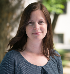
Meet Dr Amelie Heuer-Jungemann

Max Planck Institute of Biochemistry, Germany
Research project: Using DNA origami for biomedical applications
Funder: Deutsche Forschungsgemeinschaft
I’ve always been interested in how things work and amazed at natural phenomena. When I was younger, I devoured children’s science books, watched lots of science shows on TV and dreamt of one day receiving a Nobel Prize.
I had an amazing chemistry and biology teacher in high school, who inspired me to study chemistry with biochemistry. Once I started studying at university, I was hooked! It was clear that science was what I wanted to do for the rest of my life. Even standing in a smelly chemistry lab with stains all over my lab coat, I couldn’t be happier!
It’s very cool to design DNA origami and fascinating to observe the complex structures through a transmission electron microscope. Every time I see a perfectly folded structure, I get a little fuzzy feeling of happiness!
I am excited about research as I love troubleshooting problems and seeing successful results when something finally works. I hope our research will lead to the design of future therapeutics for diseases. I have many ideas, and I hope at least some of them will pave the way for positive impacts for society.
I believe there is still a lot to discover using DNA nanotechnology for biomedical, physical and computing applications, which is why, in my opinion, it is one of the most attractive fields to have a career in.
Meet Professor Tim Liedl
Faculty of Physics, Ludwig-Maximilians-Universität, Germany
Research project: Using DNA origami to construct photonic crystals
Funders: European Research Council (ERC), Deutsche Forschungsgemeinschaft, State of Bavaria
My interest in physics evolved over time. I enjoyed it in school, where physics classes were about mechanics, perhaps because I enjoyed playing with toy planes and cars and building primitive catapults.
I initially wanted to become a doctor, so I worked in a hospital to gain experience. This sparked my interest in medical equipment, so I instead chose to study physics and took classes in biophysics and medical physics, with the hope of developing ultrasound and X-ray equipment. It was only during the final year of my studies that I discovered how much I enjoyed working in a laboratory.
Usually, scientists add small pieces of understanding here and there through our research. In this way, the scientific community collectively advances knowledge of the field. The contributions of my research group to the greater field of DNA nanotechnology involve the arrangement of gold (and other metal) nanoparticles with the help of DNA origami nanostructures.
DNA nanotechnology offers rich and complex questions for physicists, chemists and biologists. How do DNA molecules build such defined structures? Can DNA nanostructures increase the activity of catalysts? Can we use DNA structures to deliver drugs to specific targets in the body?
The physics of spectroscopy
Spectroscopy is the study of the interaction of electromagnetic radiation (light) with matter. By analysing spectra of electromagnetic radiation before and after interaction with a sample, spectral changes (for example due to emission, absorption or scattering) can provide information about the sample’s composition, physical properties and structure at atomic, molecular and macro scales. Different electromagnetic wavelengths can be used to investigate different scales. For instance, X-rays provide data about individual atoms and electrons, visible light provides data about the electronic configuration of molecules, and infrared radiation provides data about molecular structure.
“Combining spectroscopy with microscopes or telescopes allows scientists to investigate from the nanoscale to astronomical distances,” says Dr Evelyn Ploetz, who uses laser light in the visible to near-infrared range to investigate how porous materials absorb and release molecules.
What research is Evelyn conducting?
Evelyn’s lab develops advanced microscopy methods, combining microscopy with spectroscopy to study how small molecules are taken up and transported in materials at the molecular level. In one project, researchers in her lab are examining gas uptake and storage in porous materials. “Droughts are an increasing problem worldwide, and metal-organic frameworks (MOFs) are a promising class of material that could harvest water from the atmosphere,” explains Evelyn. “We develop spectroscopic techniques to monitor and quantify water uptake and release from single MOF crystals to understand how materials could be designed for water harvesting.”
Another project deals with the transport of molecules, such as gases or metabolites, by porous nanoparticles into cells. “MOF nanoparticles can act as carriers in drug delivery applications due to their highly flexible designs,” says Evelyn. The team can control the design of MOFs to enter cells. However, it is not yet understood how the nanoparticles then degrade in the cell to release their cargo. “We aim to follow the chemical composition of MOF nanoparticles in cells over time to monitor their impact on cellular activity,” explains Evelyn.
What successes has Evelyn had?
Evelyn’s research group has successfully designed a new multi-modal system for optical spectroscopy and imaging that combines several spectroscopic and microscopic techniques to analyse a sample in 3D in both time and space. This is not only helping the team monitor the transport of small molecules, but has also already been used successfully to study microplastics in ocean sponges and to observe the temporal changes in the distribution of proteins in clusters of cells.
Meet Dr Evelyn Ploetz
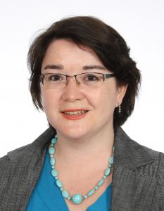
Faculty of Chemistry and Pharmacy, Ludwig-Maximilians-Universität, Germany
Research project: Using applied spectroscopy to study the transport of nanoparticles
Funder: Deutsche Forschungsgemeinschaft
I have always been a creative person with a passion for music and mathematics. It was an interest in astronomy that inspired me to study physics and become a spectroscopist. When reading about the origin of stars and galaxies at school, I learnt that spectroscopy is the tool used to monitor the composition and movement of stars. I was intrigued about how we study objects we cannot reach or touch, so I wanted to know more about spectroscopic techniques.
During my studies, I fell in love with optics. I realised how sensitive and powerful spectroscopy is for probing the structure of molecules. Light is an amazing phenomenon! It can be manipulated and combined with microscopy to non-invasively investigate the internal structure of materials. Spectroscopy is universal and applicable to many different sample systems in life sciences, material sciences and engineering.
Today, state-of-the-art spectroscopic techniques are not only used for fundamental research, but also in industries. For example, the automobile industry uses spectroscopy to inspect materials while the pharmaceutical industry uses it to characterise drugs.
The nature of nanocrystals
When was the last time you looked at a phone screen or turned on an LED lightbulb? Did you know that both these electronic devices, along with others (such as lasers and solar cells), are known as optoelectronics? “Optoelectronics are electronic devices that interact with light,” explains Professor Alexander Urban. His research group is using nanospectroscopy to investigate how halide perovskite nanocrystals can improve the efficiency and sustainability of optoelectronics.
What is nanospectroscopy?
Nanospectroscopy involves applying spectroscopic techniques at the nanoscale. “Nanoscale objects are too small to be seen with an ordinary microscope,” says Alexander. “So, in nanospectroscopy, we need to develop new ways of investigating these materials and determining how they interact with light.”
What are halide perovskite nanocrystals?
Perovskite is a crystalline mineral that contains calcium, titanium and oxygen. When part of the mineral consists of halide ions (e.g., chloride, bromide, iodide), it is known as a halide perovskite, and individual crystals exist at the nanoscale. “Halide perovskites interact very strongly with light,” explains Alexander. “They can transform sunlight into electricity or turn electricity into light of nearly any colour. Accordingly, they are nearly perfect materials for developing a new generation of more efficient and sustainable optoelectronic devices.”
What is Alexander’s research group doing?
Alexander’s research group is using nanospectroscopy and microscopy techniques to understand the properties of halide perovskite nanocrystals. This involves monitoring the light absorbed and emitted by the material and examining how energy and charge are transported in nanocrystals, which is important for understanding how to create electricity from solar cells and for making light from LEDs. “We also deposit individual nanocrystals onto substrates and cool them down to -269 °C to study their energetic structure and how it is influenced by the nanocrystals’ shape and size,” says Alexander, allowing his team to contribute to nanotechnological advances in optoelectronics.
Meet Professor Alexander Urban
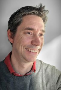
Faculty of Physics, Ludwig-Maximilians-Universität, Germany
Research project: Using nanospectroscopy to investigate the properties of halide perovskites for optoelectronics
Funders: European Research Council, Deutsche Forschungsgemeinschaft, Bavarian State Ministry of Science, Research and Arts
It was my first-grade teacher who got me excited about science and fascinated by astronomy and space exploration. While my interests have since shifted from astrophysics to solid-state physics, I still retain a strong passion for space exploration and stargazing.
The field of nanoscpectroscopy is very versatile and never gets boring! It lies at the intersection between physics, chemistry, engineering and biology, so I interact with people who approach science from many different angles. While this can be challenging, it is also rewarding, and these new perspectives lead to better results.
It is exciting to conduct research on materials that have never been made before, and to establish collaborations with colleagues around the world. Our focus on energy-related applications means this research is becoming ever-more relevant for society.
Exploring the atomic world with powerful microscopes
Have you ever looked down a microscope in your biology class to observe the features of a cell? Microscopes allow us to view the details of small things, and electron microscopes are the most powerful of all, allowing scientists to observe the tiniest details in a material. “Transmission electron microscopy allows us to view inside atoms!” says Professor Knut Müller-Caspary.
What is a transmission electron microscope?
A transmission electron microscope (TEM) fires a beam of high-energy electrons (travelling at 70% of the speed of light) at a sample. The electrons pass through the material and form an image of the sample’s internal structure. As TEM can create images with a resolution of 0.05 nm, and the bonds between atoms have a length of ~ 0.1-0.2 nm, this means TEM can observe the atomic structure of matter.
What research is Knut’s group involved in?
In Knut’s lab, his team is developing interpretations of the complex diffraction patterns that form when an electron beam inside the TEM is focused into a single atom. “We use basic quantum mechanics to relate the diffraction pattern to the electric field in the illuminated volume,” says Knut. “By scanning the electron beam across a specimen, we can measure the electric field distribution produced by the positively charged protons and the negatively charged electrons in individual atoms.”
What are the applications of TEM?
“TEM has a plethora of applications, including in nanotechnology (to determine the position and type of atoms in semiconductor optoelectronics), materials science (to characterise the atomic structure of materials) and structural biology (to uncover the molecular structure of viruses),” says Knut, highlighting how useful this technique is for increasing our understanding of matter.
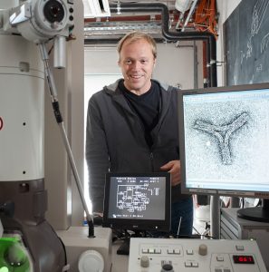
Meet Professor Knut Müller-Caspary
Faculty of Chemistry and Pharmacy, Ludwig-Maximilians- Universität, Germany
Research project: Improving transmission electron microscopy techniques for studying the atomic structure of materials
Funders: Deutsche Forschungsgemeinschaft, EQAP One Munich, Hightech Agenda of the State Bavaria
When I first used TEM, it took my supervisor a while to align all the optics of the machine and so I spent an hour watching a boring, dense fog on the screen. But then, suddenly, with a turn of the focus knob, the fog disappeared and revealed the atomic pattern of a crystal. It was amazing to see atoms in ultra-sharp definition on the screen, and my passion for resolving the atomic world has lasted since then.
TEM plays a key role in fundamental science – it is a measurement tool and a versatile nanolaboratory. It makes the most beautiful experiment of all time (the demonstration of wave-particle duality) an everyday life experience. What further reason would one need to become an electron microscopist?
It is the fascinating respect for the unknown that motivates my research group. When asked why they are passionate about science, here are some responses from my lab group members:
- “Curiosity is essential for a scientist. As a scientist, you spend every day learning new things. What more could you wish for?!”
- “I have always asked questions. Why does the sea look blue? Why does my phone battery die when it’s cold? I kept asking, and eventually reached a point where no one had an answer. That’s the moment I decided to become a scientist.”
- “Science is the key to understanding the world around us, and this knowledge then enables us to shape the world to our benefit. As a scientist, you learn things every day about how to understand and shape reality!”
ABOUT NANOSCIENCE
Get involved and learn more about nanoscience
CeNS participates in outreach events such as Munich Science Days (www.forscha.de/fo) and the nationwide Girls’ Day (www.girls-day.de). On Girls’ Day, companies and institutions open their doors to women pupils. The programme at CeNS includes visits to the labs, hands-on experiments (such as creating batteries from fruit) and career talks, all presented by women students and research group leaders to inspire and encourage girls to consider careers in fields still dominated by men.
The Max Planck Institute of Biochemistry offers the ‘Was Wissen schafft’ lecture series (www.biochem.mpg.de/en/news/publicseminars/wiss_jed). Once a month, different researchers from the institute explain their research to the public in an accessible way that everyone can understand.
The Max Planck Institute of Biochemistry also hosts the MaxLab (www.bi.mpg.de/maxlab), an interactive, hands-on science lab for school classes and visitors of all ages. The MaxLab offers courses covering different scientific topics, all related to the research currently being conducted at the institute.
The Max Planck Institute of Biochemistry has a wealth of educational resources for schools on a variety of scientific topics: www.max-wissen.de
The Faculty of Chemistry and Pharmacy at LMU organises an annual Student Information Day (www.cup.lmu.de/schuelerinfotag). School students can take guided tours of the different research labs, listen to exciting lectures from professors and students, watch researchers conducting fascinating experiments and learn about studying chemistry, biochemistry and pharmacy at LMU.
Contact the CeNS research groups (www.cens.de/research/groups) or the departments that host them if you are interested in arranging a visit or internship!
Pathway from school to nanoscience
• “A solid foundation in science and maths is essential for nanoscience,” says Susanne, so study these subjects at school.
• Some universities offer specific degree programmes in nanoscience or nanotechnology.
• As nanoscience combines physics, chemistry, biology and engineering, you can approach the field from any of these directions. Depending on your interests, you could study physics, chemistry, molecular biology, materials science or engineering to begin your career in nanoscience.
• “If you are interested in electron microscopy, you need a solid knowledge of physics, especially quantum mechanics, scattering theory, optics and electrodynamics, to understand the interaction between electrons and a specimen,” says Knut.
• “DNA nanotechnology is an incredibly interdisciplinary field,” says Amelie, “so you can study any natural or physical science subject and then get into DNA nanotechnology.”
Explore careers in nanoscience
• As a nanoscientist, you could conduct research at a university or within a company. Many industries rely on nanotechnology, so you could apply your skills to addressing challenges in pharmaceutical, biotechnology or semiconductor companies, to name just a few.
• CeNS has information about academic and non-academic careers in nanoscience: www.cens.de/careers
• This article from NanoTech News explains what nanoscientists do, where they may find themselves working, and what skills and qualifications they need: www.nanotechetc.com/nanoscientist-education-and-skills-needed-for-the-job
• Career Explorer provides information about careers in nanotechnology engineering, the branch of nanoscience that creates tiny technology: www.careerexplorer.com/careers/nanotechnology-engineer
Do you have a question for the team?
Write it in the comments box below and the team will get back to you. (Remember, researchers are very busy people, so you may have to wait a few days.)
Thanks for your valuable knowledge because of this i use to updated, thanks for sharing this wonderful article.