Extraordinarily small materials with big world applications
Professor Joshua Robinson is a materials scientist and engineer based at The Pennsylvania State University in the US. His research focuses on 2D materials, such as graphene, and he is now exploring other materials for next generation electronics
TALK LIKE A MATERIALS SCIENTIST
QUANTUM – the minimum amount of any physical entity involved in an interaction
SEMICONDUCTOR – a material with properties somewhere between an insulator and a conductor
COMPOUND SEMICONDUCTOR – a semiconductor made of more than one element on the periodic table
TWO-DIMENSIONAL (2D) MATERIALS – crystalline solids consisting of a single layer of atoms or group of atoms
GRAPHENE – a single layer of carbon atoms arranged in a 2D honeycomb nanostructure
HETEROSTRUCTURE – a layered structure in which the chemical composition changes as you move from layer-to-layer
OPTOELECTRONIC – while the majority of electronic devices are silicon based, optoelectronic devices perform their best when made using compound semiconductors made of elements from the group III and group V columns in the periodic table
SUPERCONDUCTOR – a material that conducts electricity without resistance
CHEMICAL VAPOR DEPOSITION – a technique for artificially growing thin layers of crystalline materials
“One of the superstar materials of the 21st century is graphene. Because graphene is only an atom thick, it has extraordinary properties which we could never find inside 3D materials, such as electrons that move faster than in any other material!” So says Alexander Vera, a member of Professor Joshua Robinson’s research team based at The Pennsylvania State University. When a material with such unprecedented properties is created, the scientific community is understandably excited – the potential applications are so far-reaching that there are some we cannot yet envision or comprehend… but Joshua and his team are striving to achieve them, with a view to facilitating next generation electronics.
CHANGING PROPERTIES
Typically, when traditional materials are shrunk to just a few atoms thick, they start behaving very differently – metals can become semiconductors, superconductors can work at higher temperatures, and optical materials can emit light with extraordinary efficiencies. If the team can understand and harness these materials, such phenomena can lead to far superior technologies. For instance, graphene boasts exceptional electronic properties, where electrons can travel through it like a superhighway, which is not possible with materials when they are significantly bigger.
MAKING THE ULTRA-THIN
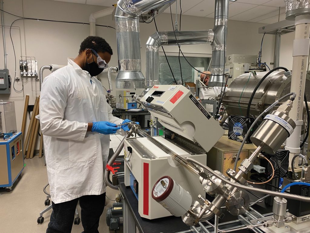
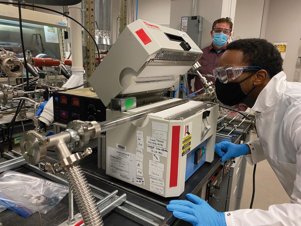
There are a lot of different ways that you can make 2D materials, from mixing powders in a blender to using multi-million-dollar technologies like molecular beam epitaxy. “Our aim is to use techniques that are industrially compatible, such as chemical vapour deposition, which is the most popular way to make semiconductors for the electronics industry,” explains Joshua. “It starts with special chemical compounds or vapours that contain the elements we want to combine, such as molybdenum and tellurium.” From there, the team puts a very small amount of those vapours into a high temperature oven. Once the oven has cooled, the substrate is removed and covered with a layer of material between one and three atoms thick!
MOVING BEYOND GRAPHENE
Graphene is considered the keystone of 2D materials, but it is only the tip of the iceberg. While graphene has tremendous properties, there are some applications it is unsuitable for, which is where large parts of the lab’s research come into play. With a focus is on the development of ‘beyond graphene’ materials, the team is seeking to uncover new materials that complement graphene or perform in entirely different ways. “Graphene is not a semiconductor – we cannot stop the electrons from flowing in graphene – so we cannot use it as a nano-switch in electronic applications, which is important since we get the ‘1s and 0s’ in computer code from these nano-switches,” says team member Cindy Chen. “There is a whole other family of 2D materials, known as transition metal dichalcogenides, that can be used in these little nano-switches, and, therefore, are more appropriate to explore for next generation electronics.”
THE CHALLENGES
Importantly, the team works closely with industry to pass on information and discoveries. Indeed, some of its industrial collaborators are already making 300mm wafers which are perfect for the electronics industry. Still, scaling up is not without its challenges, especially considering that the materials are 2D. “Everything you do to these materials impacts their properties because they are all surface!” says Joshua. “That means putting a metal or oxide on top of them changes the environment of the whole layer, not just the top surface as happens in a 3D material. Therefore, integration of these 2D layers, and understanding and controlling what happens when you sandwich them between other materials are major focuses for today’s scientists.”
KEY FINDINGS
The lab has developed methods to make 2D materials that have enabled team members to explore unique phenomena. In addition, it has discovered that when metals are squeezed down to a few atoms, they act very differently to traditional metals. One other major achievement has been the development of methods to carefully control the introduction of small amounts of impurities to 2D materials to control their electronic properties.
NEXT STEPS
“We’re constantly pushing the boundaries of making new forms of 2D materials from traditional 3D materials, and our latest is to explore what happens when you squeeze elements known as the ‘rare-earth elements’ into a 2D space,” says Joshua. “These elements are already exotic and we’re pretty sure even more weird physics is going to ‘pop-up’ when we get them in a 2D form!”
 PROFESSOR JOSHUA ROBINSON
Department of Materials Science and Engineering, Center for Atomically Thin Multifunctional Coatings, The 2D Crystal Consortium, Center for Nanoscale Science, The Pennsylvania State University, USA
FIELDS OF RESEARCH: Materials Science, Engineering
RESEARCH: Developing 2D materials, such as graphene, which boast exciting properties and have a broad range of applications within the fields of computing, energy and sensing
FUNDERS: National Science Foundation (NSF), Air Force Office of Scientific Research, Semiconductor Research Corporation, Intel, Army Research Office
Prof. Robinson’s research is possible through support from the National Science Foundation (DMR-2002651, DMR-1539916 & 2039351, IIP-2113864), The Air Force Office of Scientific Research (FA9550-19-1-0295), Semiconductor Research Corporation through the NEW LIMITS Center, and the Army Research Office (W911NF2110037)
ABOUT MATERIALS SCIENCE
Materials science is the quest to understand how materials are made and what controls their properties. As technology has developed, scientists have advanced the field to create and explore different materials with exciting – and sometimes unprecedented – properties. 2D materials, which are extremely thin (sometimes only one atom thick), form the basis of many scientific enquiries.
2D metals are an exciting avenue for exploration because of the variety of potential they offer. “Some of the applications include superconductors for quantum technologies; metasurfaces for optical computing and quantum communications; and high surface area materials for ultra-sensitive biosensors to rapidly detect viruses,” explains Joshua. “The opportunity for such materials to impact electronics lies in their ability to be combined, like LEGO blocks. 2D layers can be stacked, twisted, folded and shaped in just about any manner imaginable, making them very useful for engineering any property you like.”
Applying these materials is dependent on how you make them. “Like the rusting of a bike that has been outside for too long, 2D metals start to degrade if we aren’t careful in how we make them – because they are all surface, they can degrade almost instantly!” explains Alexander. “Part of our work is preventing that from happening, so that we can use them in electronics without fancy and expensive equipment.”
Beyond simply keeping the equipment running, one of the biggest challenges is understanding and analysing the data generated. Researchers must link data back to how the material was made. “Often, we will make a material and it will perform in a certain way, but we don’t know why,” says Cindy. “That’s when we have to rely on the science community around us to dive a bit deeper into the analysis or theoretically model the behaviour to help us understand.”
EXPLORE CAREERS IN MATERIALS SCIENCE
• The best advice Joshua can give to budding students is to get into a lab and explore! “Seek out internships, summer
programmes, or even volunteer at a local college/university lab – it’s the best way to identify what you enjoy in the sciences,” says Joshua.
• Joshua is part of the Center for Nanoscale Science. Explore the outreach programmes.
• The US Bureau of Labor Statistics has useful information about careers in material science. It states the average salary of a materials scientist in the US as $104,000.
• According to Payscale.com, the average salary for a materials scientist in the UK is £32,000.
Reference
https://doi.org/10.33424/FUTURUM260


QUANTUM – the minimum amount of any physical entity involved in an interaction
SEMICONDUCTOR – a material with properties somewhere between an insulator and a conductor
COMPOUND SEMICONDUCTOR – a semiconductor made of more than one element on the periodic table
TWO-DIMENSIONAL (2D) MATERIALS – crystalline solids consisting of a single layer of atoms or group of atoms
GRAPHENE – a single layer of carbon atoms arranged in a 2D honeycomb nanostructure
HETEROSTRUCTURE – a layered structure in which the chemical composition changes as you move from layer-to-layer
OPTOELECTRONIC – while the majority of electronic devices are silicon based, optoelectronic devices perform their best when made using compound semiconductors made of elements from the group III and group V columns in the periodic table
SUPERCONDUCTOR – a material that conducts electricity without resistance
CHEMICAL VAPOR DEPOSITION – a technique for artificially growing thin layers of crystalline materials
“One of the superstar materials of the 21st century is graphene. Because graphene is only an atom thick, it has extraordinary properties which we could never find inside 3D materials, such as electrons that move faster than in any other material!” So says Alexander Vera, a member of Professor Joshua Robinson’s research team based at The Pennsylvania State University. When a material with such unprecedented properties is created, the scientific community is understandably excited – the potential applications are so far-reaching that there are some we cannot yet envision or comprehend… but Joshua and his team are striving to achieve them, with a view to facilitating next generation electronics.
CHANGING PROPERTIES
Typically, when traditional materials are shrunk to just a few atoms thick, they start behaving very differently – metals can become semiconductors, superconductors can work at higher temperatures, and optical materials can emit light with extraordinary efficiencies. If the team can understand and harness these materials, such phenomena can lead to far superior technologies. For instance, graphene boasts exceptional electronic properties, where electrons can travel through it like a superhighway, which is not possible with materials when they are significantly bigger.
MAKING THE ULTRA-THIN
There are a lot of different ways that you can make 2D materials, from mixing powders in a blender to using multi-million-dollar technologies like molecular beam epitaxy. “Our aim is to use techniques that are industrially compatible, such as chemical vapour deposition, which is the most popular way to make semiconductors for the electronics industry,” explains Joshua. “It starts with special chemical compounds or vapours that contain the elements we want to combine, such as molybdenum and tellurium.” From there, the team puts a very small amount of those vapours into a high temperature oven. Once the oven has cooled, the substrate is removed and covered with a layer of material between one and three atoms thick!
MOVING BEYOND GRAPHENE
Graphene is considered the keystone of 2D materials, but it is only the tip of the iceberg. While graphene has tremendous properties, there are some applications it is unsuitable for, which is where large parts of the lab’s research come into play. With a focus is on the development of ‘beyond graphene’ materials, the team is seeking to uncover new materials that complement graphene or perform in entirely different ways. “Graphene is not a semiconductor – we cannot stop the electrons from flowing in graphene – so we cannot use it as a nano-switch in electronic applications, which is important since we get the ‘1s and 0s’ in computer code from these nano-switches,” says team member Cindy Chen. “There is a whole other family of 2D materials, known as transition metal dichalcogenides, that can be used in these little nano-switches, and, therefore, are more appropriate to explore for next generation electronics.”
THE CHALLENGES
Importantly, the team works closely with industry to pass on information and discoveries. Indeed, some of its industrial collaborators are already making 300mm wafers which are perfect for the electronics industry. Still, scaling up is not without its challenges, especially considering that the materials are 2D. “Everything you do to these materials impacts their properties because they are all surface!” says Joshua. “That means putting a metal or oxide on top of them changes the environment of the whole layer, not just the top surface as happens in a 3D material. Therefore, integration of these 2D layers, and understanding and controlling what happens when you sandwich them between other materials are major focuses for today’s scientists.”
KEY FINDINGS
The lab has developed methods to make 2D materials that have enabled team members to explore unique phenomena. In addition, it has discovered that when metals are squeezed down to a few atoms, they act very differently to traditional metals. One other major achievement has been the development of methods to carefully control the introduction of small amounts of impurities to 2D materials to control their electronic properties.
NEXT STEPS
“We’re constantly pushing the boundaries of making new forms of 2D materials from traditional 3D materials, and our latest is to explore what happens when you squeeze elements known as the ‘rare-earth elements’ into a 2D space,” says Joshua. “These elements are already exotic and we’re pretty sure even more weird physics is going to ‘pop-up’ when we get them in a 2D form!”
However, this is an extremely straightforward example. “The complexity of the problem is exciting,” says Justin. “For instance, if you draw 25 dots on a piece of paper to represent the points in a graph, and then attempt to connect them using every possible combination of links, the number of graphs you could construct is larger than the number of atoms in the known universe.” It is possible to use mathematical rules to reduce this complexity to something manageable for basic smartphones or laptops. Justin’s team is working on developing a tool for the visual representation of graph compression algorithms. They aim to make such tools more user-friendly for the real world.
PROFESSOR JOSHUA ROBINSON
Department of Materials Science and Engineering, Center for Atomically Thin Multifunctional Coatings, The 2D Crystal Consortium, Center for Nanoscale Science, The Pennsylvania State University, USA
FIELDS OF RESEARCH: Materials Science, Engineering
RESEARCH: Developing 2D materials, such as graphene, which boast exciting properties and have a broad range of applications within the fields of computing, energy and sensing
FUNDERS: National Science Foundation (NSF), Air Force Office of Scientific Research, Semiconductor Research Corporation, Intel, Army Research Office
Prof. Robinson’s research is possible through support from the National Science Foundation (DMR-2002651, DMR-1539916 & 2039351, IIP-2113864), The Air Force Office of Scientific Research (FA9550-19-1-0295), Semiconductor Research Corporation through the NEW LIMITS Center, and the Army Research Office (W911NF2110037)
ABOUT MATERIALS SCIENCE
Materials science is the quest to understand how materials are made and what controls their properties. As technology has developed, scientists have advanced the field to create and explore different materials with exciting – and sometimes unprecedented – properties. 2D materials, which are extremely thin (sometimes only one atom thick), form the basis of many scientific enquiries.
2D metals are an exciting avenue for exploration because of the variety of potential they offer. “Some of the applications include superconductors for quantum technologies; metasurfaces for optical computing and quantum communications; and high surface area materials for ultra-sensitive biosensors to rapidly detect viruses,” explains Joshua. “The opportunity for such materials to impact electronics lies in their ability to be combined, like LEGO blocks. 2D layers can be stacked, twisted, folded and shaped in just about any manner imaginable, making them very useful for engineering any property you like.”
Applying these materials is dependent on how you make them. “Like the rusting of a bike that has been outside for too long, 2D metals start to degrade if we aren’t careful in how we make them – because they are all surface, they can degrade almost instantly!” explains Alexander. “Part of our work is preventing that from happening, so that we can use them in electronics without fancy and expensive equipment.”
Beyond simply keeping the equipment running, one of the biggest challenges is understanding and analysing the data generated. Researchers must link data back to how the material was made. “Often, we will make a material and it will perform in a certain way, but we don’t know why,” says Cindy. “That’s when we have to rely on the science community around us to dive a bit deeper into the analysis or theoretically model the behaviour to help us understand.”
EXPLORE CAREERS IN MATERIALS SCIENCE
• The best advice Joshua can give to budding students is to get into a lab and explore! “Seek out internships, summer
programmes, or even volunteer at a local college/university lab – it’s the best way to identify what you enjoy in the sciences,” says Joshua.
• Joshua is part of the Center for Nanoscale Science. Explore the outreach programmes.
• The US Bureau of Labor Statistics has useful information about careers in material science. It states the average salary of a materials scientist in the US as $104,000.
• According to Payscale.com, the average salary for a materials scientist in the UK is £32,000.
PATHWAY FROM SCHOOL TO MATERIALS SCIENCE
Joshua recommends taking physics, chemistry and mathematics at school and college. “Materials science is all about the world of materials – how they are made, how they function and how they can be utilised,” he explains. “Understanding the basic physics and chemistry ‘languages’ is critical to being able to dive into the world of materials.”
You will normally need a minimum of a bachelor’s (foundation) degree, with many semiconductor or electronic industries most interested in master’s or PhD degrees. Relevant subjects include materials engineering, materials science, chemistry and solid-state physics, and electrical engineering.
Alexander explains, “Materials science is a broad discipline which can touch on so many fields. So, depending on which path you take, subjects like food science and forensic science could also be useful – you could even end up working on food packaging or be part of a legal case as a materials scientist!”
HOW DID JOSHUA BECOME A MATERIALS SCIENTIST?
I had many interests growing up and was fascinated about the world around me. My brother and I were always exploring, which I believe is a key ingredient in the way I go about life today. Now, instead of picking up rocks in a creek to see what’s underneath, I peel up graphene to look at the atoms!
My route into science is thanks to my encouraging parents and a great undergraduate mentor. Growing up, I was always curious, but the experiences I had as an undergraduate student were perhaps what sent me down the path of scientific exploration rather than any other. Professor David Schaefer (Towson University) gave me a great opportunity to ‘play’ in his lab and learn about nanoscale materials.
It’s incredibly satisfying to see my students succeed. The research is exciting, and we seem to be discovering new things on a regular basis, but it’s the people that I am surrounded by that gets me up and keeps me going every day. I especially enjoy when a student finally ‘gets it’ and then starts coming to me with ideas to explore – that means they are thinking at a higher level, and sometimes a few levels higher than I am, which means it’s time for them to graduate!
The possibilities for the impact of 2D materials are wide open. There are so many possible applications, from 2D materials in composites for better performing tyres, all the way to advanced nanoscale heterostructures for quantum computing. This provides the opportunity for students to work in a broad spectrum of industry, academia and government.
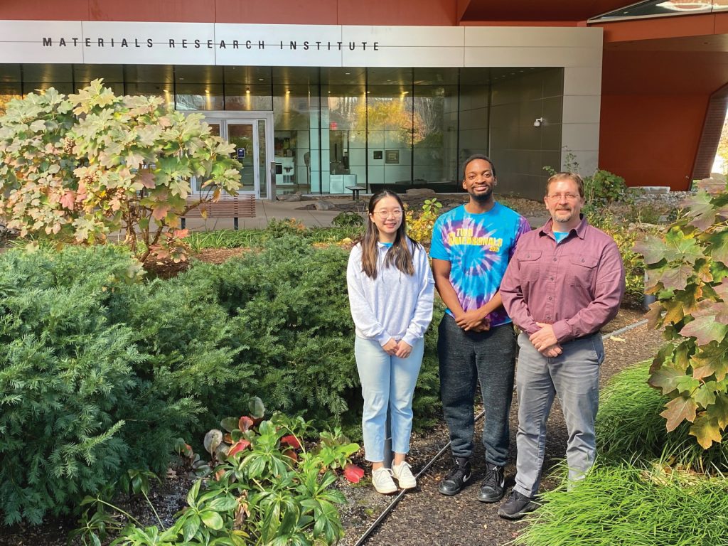
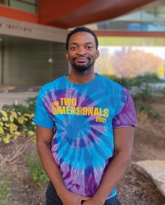
MEET ALEXANDER VERA
I am a researcher, working on the synthesis of ultra-thin metals, and a safety officer. My day is spent in Joshua’s lab performing experiments, writing manuscripts or engaging in outreach activities.
I enjoyed physics in high school, so I opted for an applied physics degree for my bachelor’s. My department was interdisciplinary, so I was introduced to materials science. My undergrad department was also known for 2D materials research, which led to my choosing to work in this unique field.
Growing up, I was always interested in marine life and astronomy. However, I also loved storytelling, fables and fantasy. I liked to play historical strategy games as well!
When I was younger, I rarely saw my identities reflected in my fellow classmates or my instructors. I saw how I was privileged to follow my passion where others like me were not, so I wanted to inspire others to pursue STEM fields.
I can attribute my success in science to patience, listening and creativity. We are given many problems to tackle, not just in the lab, but throughout the whole scientific career. At every problem, surprisingly, my love for storytelling has lent me these attributes and helped me find solutions.
In 2020, I was accepted to the Sloan Foundation, which recognises active students of colour in higher education. With some of the funds awarded, I was able to travel to Oak Ridge National Labs for a week-long site visit, which was exciting!
One of my chief aims in the future is to graduate from Penn State with a PhD. I very much hope to continue working in science and nanotechnology, with a focus on diversity, equity and inclusion.
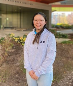
MEET CINDY CHEN
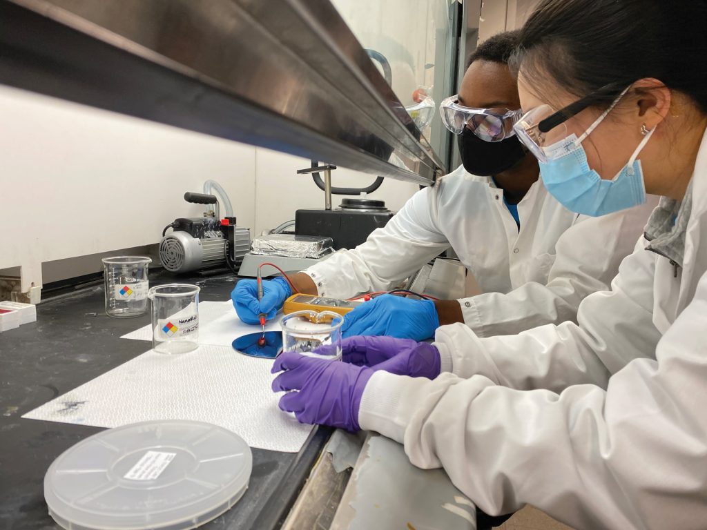
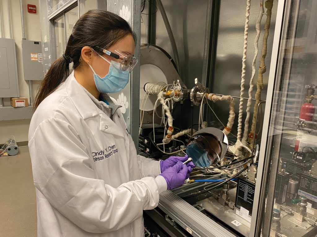
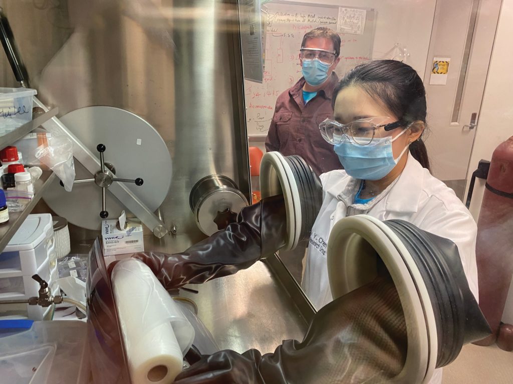
I design experiments for the synthesis of 2D materials and oversee one of the deposition tools we use to grow materials. I am also a lab manager, so I train new users and make sure they are always safe around the lab.
Most of the time, I work in the lab and conduct experiments. After materials growth, I take my materials to analytical instruments so I can understand their structures and chemistries better. Some days, I work in the cleanroom, suited up from head to toe to ensure I don’t contaminate our samples.
I majored in materials science, and one of my favourite courses was on the electronic properties of materials. This led me to join a research group and present my undergraduate research at a conference, which was where I met the members of the group I currently work in.
I was a part of my high school’s Science Olympiad and Science Bowl teams. It was refreshing to learn new science topics not taught in class, and, more importantly, it was fun. Outside of school, I enjoyed teaching clay art alongside my mom, who is an art teacher.
My high school physics teacher, Mr Slattery, was my biggest inspiration. He always believed in me, even when I lost confidence in myself. I keep in touch with him to this day.
Once I set my mind on something, I am determined to achieve my goals. Failures are lessons for becoming a better scientist!
I am proud that I finally optimised the recipe for growing 2D semiconducting molybdenum ditelluride. This was challenging, with many failed experiments and broken tool parts, but I never gave up and was determined to make the material a reality.
My aim is to work as an engineer in the semiconductor industry, to be part of a team designing the next generation of new electronic technologies.
01 We fail more often than we succeed. The key is not to run from failure, but to learn and grow from it. If you do this, you will succeed many times!
02 Be creative and stay true to yourself. So much of science is about novelty, which cannot happen without your unique human experience.
03 Find what you love to do and don’t be afraid to put all of yourself into it. It is also important to identify and maintain a supportive network of friends, family and mentors, and support them in the same way as they support you.
Do you have a question for Joshua, Alex or Cindy?
Write it in the comments box below and Joshua, Alex or Cindy will get back to you. (Remember, researchers are very busy people, so you may have to wait a few days.)