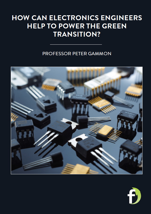
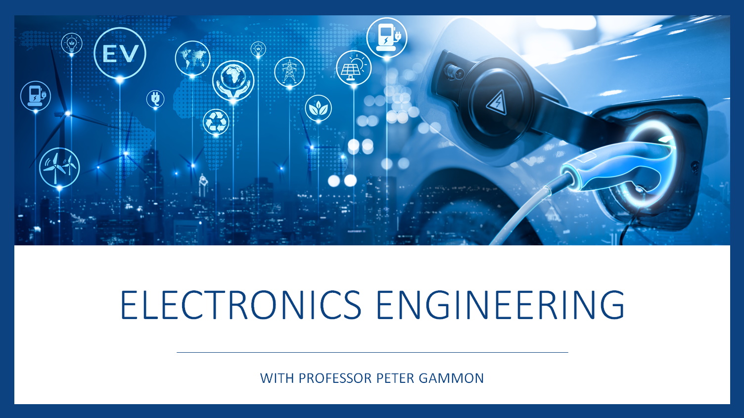
How can electronics engineers help to power the green transition?
TALK LIKE AN ELECTRONICS ENGINEER
ALTERNATING CURRENT (AC) – electrical current which reverses direction periodically. Electricity is transported to your home as AC
DIRECT CURRENT (DC) – electrical current which only flows in one direction. Most of your gadgets run on DC
NATIONAL GRID – the network and infrastructure that produces electricity and distributes it to consumers
SEMICONDUCTOR – a material which is an insulator at low temperatures but an electrical conductor at high temperatures
TRANSISTOR – a component of electrical circuits which switches between AC and DC
Increasing our production of renewable energy will help to reduce our carbon emissions, yet up to 10% of all renewable energy generated is wasted before it even reaches your phone, laptop or lightbulbs. At each stage of transporting this electricity, from wind farm to National Grid to your house to your phone, a small amount of electricity is wasted as it heats up the transistors it travels through. If we could make these transistors more efficient, less energy would be wasted. And that is what Peter is trying to achieve.
WHAT IS A TRANSISTOR?
“A transistor is an electrical switch – much like a light switch,” Peter explains. Traditionally made from silicon, a cheap but not very efficient semiconductor, transistors are the key components of modern electronics and have enabled the massive growth in computing over recent decades. Without transistors, the modern world would be a very different place!
Peter likes to use the analogy of a dam across a river to describe how a transistor functions. “The purpose of the dam is to turn the flow of water downstream from the reservoir above on and off, whilst the purpose of the transistor is to turn the flow of electrical current downstream from a battery on and off.” Using this same analogy, the voltage of the battery corresponds to the water pressure behind the dam. Peter and his team are focused on designing and building transistors. “It is our job as designers of transistors to make them more efficient, so that we waste less of the power we generate,” explains Peter. And to do this, he is creating them out of silicon carbide.
THE NEW SUPER MATERIAL
Silicon carbide is a compound formed from alternating atoms of silicon and carbon arranged in a hexagonal crystal pattern. It is relatively common in outer space but is extremely rare on Earth – the first time silicon carbide was detected naturally was in the remnants of a meteorite! All the silicon carbide we use on Earth is synthetic. It has been manufactured for use in bulletproof vests, as brake discs in super cars, as an alternative to diamonds in jewellery and even as the abrasive surface on skateboards.
In recent decades, engineers have started to use silicon carbide as a semiconductor, where it has several advantages over pure silicon when used for power electronics. Peter returns to the dam analogy to explain. “Building a transistor out of silicon carbide rather than silicon is like building a dam out of reinforced concrete rather than regular concrete,” he says. “The extra-strong reinforced concrete allows us to hold back the same volume of water with a thinner dam – similarly, the use of silicon carbide allows us to withstand the same battery voltage with a thinner semiconductor.” In turn, thinner semiconductors make for transistors which can operate with lower resistance, thereby improving efficiency.
An example of this has occurred in the manufacture of electric cars. Transistors in the car’s power converter transform the DC electricity stored in the battery to AC electricity which is needed by the car’s motor. Tesla was the first company to replace silicon transistors with silicon carbide ones, making its converter significantly more efficient than it was before. By wasting less energy, the car can travel further before it needs to be recharged, or the number of heavy, expensive batteries the car needs can be reduced.
HOW DOES PETER MANUFACTURE HIS SILICON CARBIDE TRANSISTORS?
Sophisticated engineering is required to develop the electrical circuitry which will power the green transition. This is highly interdisciplinary work, involving electronics engineering, electrical engineering and materials science.
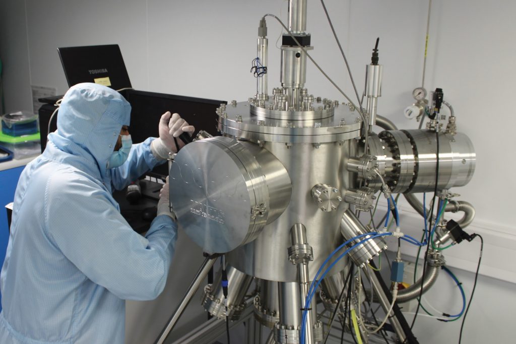
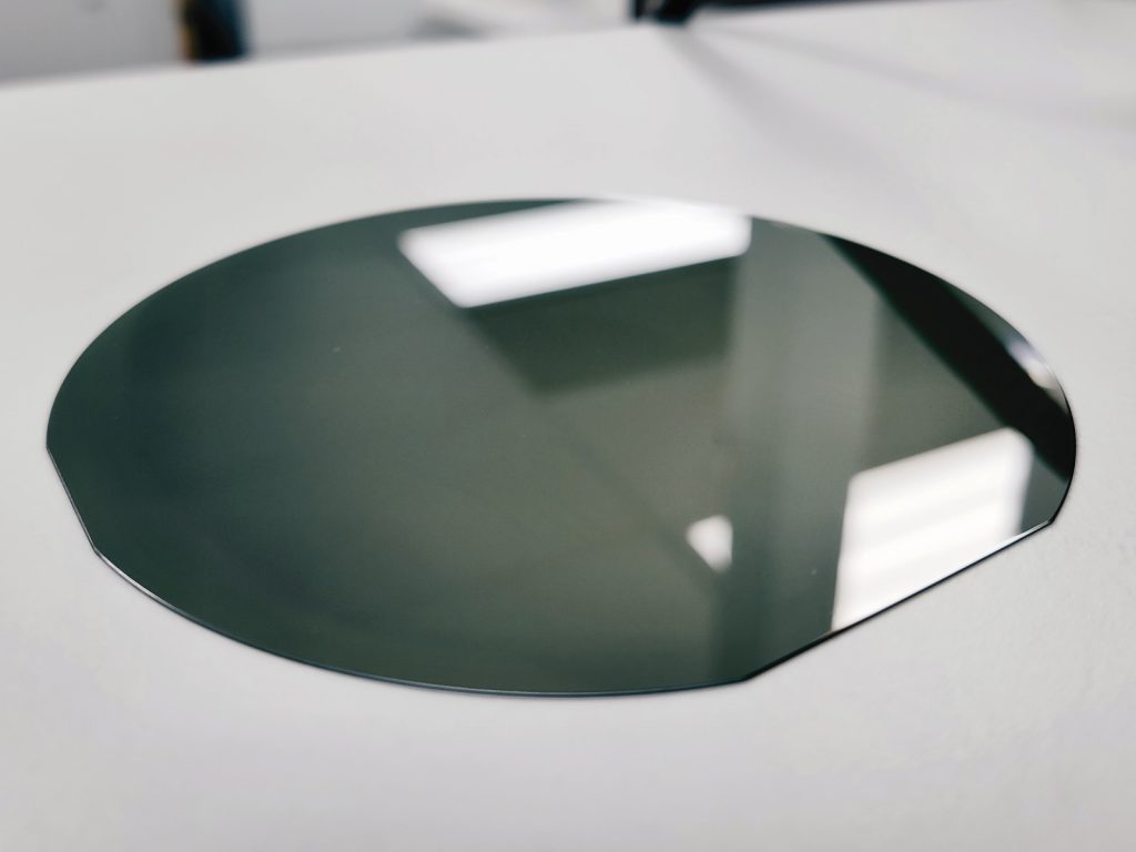
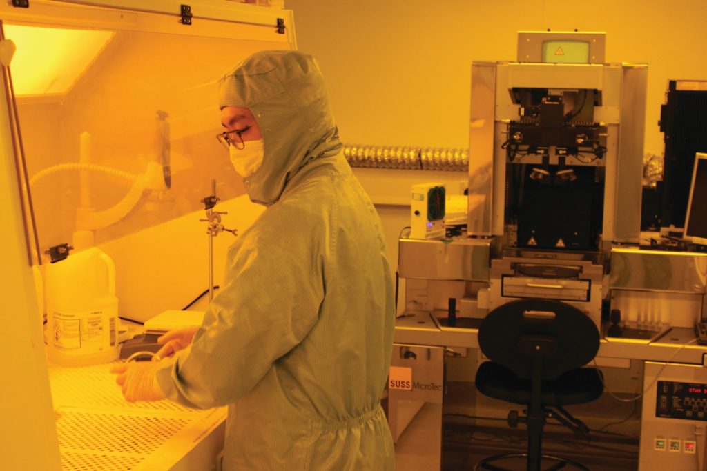
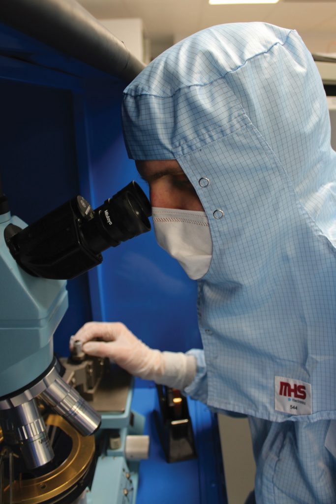
To make his silicon carbide transistors, Peter begins with a very thin circular wafer of silicon carbide that is 100 mm in diameter and less than half a millimetre thick. “Making the transistors on top of this wafer is a process involving up to 20 individual steps,” he says, “each of which changes the way that current flows through the material.” These steps include growing more silicon carbide on the surface of the wafer, using a process called epitaxy, then oxidising these surfaces, depositing metals and etching trenches in them. This is microscopic engineering, involving physical and chemical changes on a scale of less than one thousandth of a millimetre. Working in a cleanroom to ensure the electronics remain absolutely spotless, Peter and his team can produce hundreds of transistor chips on a single silicon carbide wafer. These are then cut up and individually packaged, ready to sell to manufacturers for use in electronic devices.
SILICON CARBIDE ON SATELLITES
As well as its use in electric vehicles, silicon carbide can be used in many other high voltage electronic systems to increase efficiency and so reduce wasted energy. This includes powering data centres, in robotics and in the infrastructure of the National Grid itself. Peter is particularly interested in the application of silicon carbide in the electronics contained on satellites.
But there are particular challenges when working with electronics in space. “The Earth’s atmosphere protects us from a universe full of radiation, with only a few parts of the electromagnetic spectrum – such as visible light – getting through it unimpeded,” Peter explains. “But outside of our atmosphere, our satellites must work under constant bombardment of energised particles.” This radiation can interfere with the electronic systems onboard satellites, so Peter and his team are researching how to ensure their transistors are protected from radiation bombardment.
There are over 2000 communications satellites in orbit around the Earth, transmitting and receiving data for satellite TV, international phone calls and credit card payments. Getting each one of these satellites into space requires a huge amount of preparation and resources – and money. By replacing the silicon in the satellite electronics with silicon carbide, Peter hopes to decrease the number of satellites that need to be launched, thereby reducing costs and also reducing the amount of resources needed, again contributing to a greener future.
Not only will silicon carbide increase the efficiency of the electronics, but it can also work at a higher temperature than silicon. This will allow the power electronics to sit next to the very hot radiofrequency amplifiers in the satellite that they supply power to. This would free up a lot of space in the satellite, meaning that each satellite could hold more communication channels, meaning we would need fewer of them.
Silicon carbide is also being used in a new generation of small satellites to work on Earth observation. Monitoring climate change requires large numbers of satellites to orbit around the Earth, recording data on everything from ocean colour to glacial retreat. Just as it is replacing silicon in transistors, silicon carbide is also starting to replace aluminium or glass in the mirrors that satellites use to collect their images. So, it turns out that whether you want to drive the green transition by developing innovative technology or by observing the impacts of climate change, you could find a career working with silicon carbide!
 PROFESSOR PETER GAMMON
Professor of Power Electronic Devices, University of Warwick, UK
FIELDS OF RESEARCH: Electronics Engineering, Electrical Engineering, Materials Science
RESEARCH PROJECT: Developing silicon carbide technology for electric vehicles, satellites and the National Grid
FUNDER: Engineering and Physical Sciences Research Council (This work was supported by the EPSRC, under award number EP/V000543/1, the SiCSat Project.)
ABOUT ELECTRONICS ENGINEERING
WHAT IS THE DIFFERENCE BETWEEN ELECTRONICS ENGINEERING AND ELECTRICAL ENGINEERING?
In general, electronics engineers are focused on the small-scale circuitry within individual electronic devices, while electrical engineers are concerned with how electricity is moved over larger distances, such as in power systems or motors. However, this distinction is often blurred. “In our group we use techniques from electronics engineering and materials science to solve electrical engineering problems,” explains Peter. “So, any good systems designer needs to have a very broad knowledge base. I believe that today’s interconnectedness of our lives with technology makes this kind of interdisciplinarity essential.”
WHAT ARE THE JOYS OF ELECTRONICS ENGINEERING RESEARCH?
Designing and carrying out electronics experiments can be great fun, but it takes a long time. While some researchers prefer this aspect of the work, Peter enjoys examining the results of experiments. “I love nothing more than the moment when I get to sit down with the data to find out if the idea we had at the start of the project – usually months before – worked,” says Peter. “Often, it hasn’t! Some people love the making, the writing up, or the story telling after, but for me the best bit is getting stuck into the numbers as they give up their secrets.”
As with other fields of science, electronics and electrical engineering offer plenty of scope for international collaboration. “I am privileged to be able to go across the world, to Japan, Europe and the US, to discuss my scientific ideas with interesting people,” Peter adds.
WHAT ISSUES WILL FACE THE NEXT GENERATION OF ELECTRONICS ENGINEERS?
“Throughout the 21st century electronics and electrical engineers will play a big role in the electrification of every system that previously required fossil fuels to be burnt,” Peter says. While this process is gaining momentum in electric cars and trains, other transport sectors such as shipping and aircraft are still a long way from being able to operate free of fossil fuels. The field of electronics engineering will be at the forefront of designing the technology for the green transition.
EXPLORE A CAREER IN ELECTRONICS ENGINEERING
• The Institute of Electrical and Electronics Engineers (www.ieee.org) and the Institution of Engineering and Technology (www.theiet.org) are dedicated to electronics engineering and the wider field of technology.
• The IET has a section of their website dedicated to careers in engineering and technology (www.theiet.org/career), as well as information for students (www.theiet.org/career/routes-to-engineering/student-hub) and advice about apprenticeships (www.theiet.org/career/routes-to-engineering/apprenticeships/introducing-apprenticeships/find-an-apprenticeship).
• The National Careers Service has information about how to become an electronics engineer and what the job may involve (nationalcareers.service.gov.uk/job-profiles/electronics-engineer).
• With a degree in electronics engineering, you could find yourself designing an iPhone, the next Tesla or even an electric aeroplane! Or you could be at the forefront of the green revolution, developing solar cells, wind farms or nuclear fusion reactors. The opportunities for electronics engineers are endless!
Reference
https://doi.org/10.33424/FUTURUM227


ALTERNATING CURRENT (AC) – electrical current which reverses direction periodically. Electricity is transported to your home as AC
DIRECT CURRENT (DC) – electrical current which only flows in one direction. Most of your gadgets run on DC
NATIONAL GRID – the network and infrastructure that produces electricity and distributes it to consumers
SEMICONDUCTOR – a material which is an insulator at low temperatures but an electrical conductor at high temperatures
TRANSISTOR – a component of electrical circuits which switches between AC and DC
Increasing our production of renewable energy will help to reduce our carbon emissions, yet up to 10% of all renewable energy generated is wasted before it even reaches your phone, laptop or lightbulbs. At each stage of transporting this electricity, from wind farm to National Grid to your house to your phone, a small amount of electricity is wasted as it heats up the transistors it travels through. If we could make these transistors more efficient, less energy would be wasted. And that is what Peter is trying to achieve.
WHAT IS A TRANSISTOR?
“A transistor is an electrical switch – much like a light switch,” Peter explains. Traditionally made from silicon, a cheap but not very efficient semiconductor, transistors are the key components of modern electronics and have enabled the massive growth in computing over recent decades. Without transistors, the modern world would be a very different place!
Peter likes to use the analogy of a dam across a river to describe how a transistor functions. “The purpose of the dam is to turn the flow of water downstream from the reservoir above on and off, whilst the purpose of the transistor is to turn the flow of electrical current downstream from a battery on and off.” Using this same analogy, the voltage of the battery corresponds to the water pressure behind the dam. Peter and his team are focused on designing and building transistors. “It is our job as designers of transistors to make them more efficient, so that we waste less of the power we generate,” explains Peter. And to do this, he is creating them out of silicon carbide.
THE NEW SUPER MATERIAL
Silicon carbide is a compound formed from alternating atoms of silicon and carbon arranged in a hexagonal crystal pattern. It is relatively common in outer space but is extremely rare on Earth – the first time silicon carbide was detected naturally was in the remnants of a meteorite! All the silicon carbide we use on Earth is synthetic. It has been manufactured for use in bulletproof vests, as brake discs in super cars, as an alternative to diamonds in jewellery and even as the abrasive surface on skateboards.
In recent decades, engineers have started to use silicon carbide as a semiconductor, where it has several advantages over pure silicon when used for power electronics. Peter returns to the dam analogy to explain. “Building a transistor out of silicon carbide rather than silicon is like building a dam out of reinforced concrete rather than regular concrete,” he says. “The extra-strong reinforced concrete allows us to hold back the same volume of water with a thinner dam – similarly, the use of silicon carbide allows us to withstand the same battery voltage with a thinner semiconductor.” In turn, thinner semiconductors make for transistors which can operate with lower resistance, thereby improving efficiency.
An example of this has occurred in the manufacture of electric cars. Transistors in the car’s power converter transform the DC electricity stored in the battery to AC electricity which is needed by the car’s motor. Tesla was the first company to replace silicon transistors with silicon carbide ones, making its converter significantly more efficient than it was before. By wasting less energy, the car can travel further before it needs to be recharged, or the number of heavy, expensive batteries the car needs can be reduced.
HOW DOES PETER MANUFACTURE HIS SILICON CARBIDE TRANSISTORS?
Sophisticated engineering is required to develop the electrical circuitry which will power the green transition. This is highly interdisciplinary work, involving electronics engineering, electrical engineering and materials science.
To make his silicon carbide transistors, Peter begins with a very thin circular wafer of silicon carbide that is 100 mm in diameter and less than half a millimetre thick. “Making the transistors on top of this wafer is a process involving up to 20 individual steps,” he says, “each of which changes the way that current flows through the material.” These steps include growing more silicon carbide on the surface of the wafer, using a process called epitaxy, then oxidising these surfaces, depositing metals and etching trenches in them. This is microscopic engineering, involving physical and chemical changes on a scale of less than one thousandth of a millimetre. Working in a cleanroom to ensure the electronics remain absolutely spotless, Peter and his team can produce hundreds of transistor chips on a single silicon carbide wafer. These are then cut up and individually packaged, ready to sell to manufacturers for use in electronic devices.
SILICON CARBIDE ON SATELLITES
As well as its use in electric vehicles, silicon carbide can be used in many other high voltage electronic systems to increase efficiency and so reduce wasted energy. This includes powering data centres, in robotics and in the infrastructure of the National Grid itself. Peter is particularly interested in the application of silicon carbide in the electronics contained on satellites.
But there are particular challenges when working with electronics in space. “The Earth’s atmosphere protects us from a universe full of radiation, with only a few parts of the electromagnetic spectrum – such as visible light – getting through it unimpeded,” Peter explains. “But outside of our atmosphere, our satellites must work under constant bombardment of energised particles.” This radiation can interfere with the electronic systems onboard satellites, so Peter and his team are researching how to ensure their transistors are protected from radiation bombardment.
There are over 2000 communications satellites in orbit around the Earth, transmitting and receiving data for satellite TV, international phone calls and credit card payments. Getting each one of these satellites into space requires a huge amount of preparation and resources – and money. By replacing the silicon in the satellite electronics with silicon carbide, Peter hopes to decrease the number of satellites that need to be launched, thereby reducing costs and also reducing the amount of resources needed, again contributing to a greener future.
Not only will silicon carbide increase the efficiency of the electronics, but it can also work at a higher temperature than silicon. This will allow the power electronics to sit next to the very hot radiofrequency amplifiers in the satellite that they supply power to. This would free up a lot of space in the satellite, meaning that each satellite could hold more communication channels, meaning we would need fewer of them.
Silicon carbide is also being used in a new generation of small satellites to work on Earth observation. Monitoring climate change requires large numbers of satellites to orbit around the Earth, recording data on everything from ocean colour to glacial retreat. Just as it is replacing silicon in transistors, silicon carbide is also starting to replace aluminium or glass in the mirrors that satellites use to collect their images. So, it turns out that whether you want to drive the green transition by developing innovative technology or by observing the impacts of climate change, you could find a career working with silicon carbide!
PROFESSOR PETER GAMMONProfessor of Power Electronic Devices, University of Warwick, UK
FIELDS OF RESEARCH: Electronics Engineering, Electrical Engineering, Materials Science
RESEARCH PROJECT: Developing silicon carbide technology for electric vehicles, satellites and the National Grid
FUNDER: Engineering and Physical Sciences Research Council (This work was supported by the EPSRC, under award number EP/V000543/1, the SiCSat Project.)
WHAT IS THE DIFFERENCE BETWEEN ELECTRONICS ENGINEERING AND ELECTRICAL ENGINEERING?
In general, electronics engineers are focused on the small-scale circuitry within individual electronic devices, while electrical engineers are concerned with how electricity is moved over larger distances, such as in power systems or motors. However, this distinction is often blurred. “In our group we use techniques from electronics engineering and materials science to solve electrical engineering problems,” explains Peter. “So, any good systems designer needs to have a very broad knowledge base. I believe that today’s interconnectedness of our lives with technology makes this kind of interdisciplinarity essential.”
WHAT ARE THE JOYS OF ELECTRONICS ENGINEERING RESEARCH?
Designing and carrying out electronics experiments can be great fun, but it takes a long time. While some researchers prefer this aspect of the work, Peter enjoys examining the results of experiments. “I love nothing more than the moment when I get to sit down with the data to find out if the idea we had at the start of the project – usually months before – worked,” says Peter. “Often, it hasn’t! Some people love the making, the writing up, or the story telling after, but for me the best bit is getting stuck into the numbers as they give up their secrets.”
As with other fields of science, electronics and electrical engineering offer plenty of scope for international collaboration. “I am privileged to be able to go across the world, to Japan, Europe and the US, to discuss my scientific ideas with interesting people,” Peter adds.
WHAT ISSUES WILL FACE THE NEXT GENERATION OF ELECTRONICS ENGINEERS?
“Throughout the 21st century electronics and electrical engineers will play a big role in the electrification of every system that previously required fossil fuels to be burnt,” Peter says. While this process is gaining momentum in electric cars and trains, other transport sectors such as shipping and aircraft are still a long way from being able to operate free of fossil fuels. The field of electronics engineering will be at the forefront of designing the technology for the green transition.
EXPLORE A CAREER IN ELECTRONICS ENGINEERING
• The Institute of Electrical and Electronics Engineers (www.ieee.org) and the Institution of Engineering and Technology (www.theiet.org) are dedicated to electronics engineering and the wider field of technology.
• The IET has a section of their website dedicated to careers in engineering and technology (www.theiet.org/career), as well as information for students (www.theiet.org/career/routes-to-engineering/student-hub) and advice about apprenticeships (www.theiet.org/career/routes-to-engineering/apprenticeships/introducing-apprenticeships/find-an-apprenticeship).
• The National Careers Service has information about how to become an electronics engineer and what the job may involve (nationalcareers.service.gov.uk/job-profiles/electronics-engineer).
• With a degree in electronics engineering, you could find yourself designing an iPhone, the next Tesla or even an electric aeroplane! Or you could be at the forefront of the green revolution, developing solar cells, wind farms or nuclear fusion reactors. The opportunities for electronics engineers are endless!
PATHWAY FROM SCHOOL TO ELECTRONICS ENGINEER
• A strong background in the sciences, maths and computing is useful in electronics engineering, but Peter also advises that good English language skills are essential for communicating about your work and writing scientific reports.
• Maths, physics, computer science and chemistry are good options to study at A-level. “But don’t rule out doing that ‘extra’ subject in something different to keep your options open,” suggests Peter.
• Many universities offer degrees in electronics engineering, but other courses may also cover aspects of electronics, including aerospace engineering, physics, nanotechnology and computer science.
• College and university are not the only routes to becoming an electronics engineer. “Apprenticeships may offer you a good alternative route if you want a more hands-on experience than college will offer you,” says Peter. He left school at 16 to do an apprenticeship in industry, learning electronics engineering straight from school.
HOW DID PETER BECOME AN ELECTRONICS ENGINEER?
AS SOMEONE WHO DESIGNS ELECTRONICS, ARE YOU A ‘GADGET PERSON’ OUTSIDE OF WORK?
Yes! I am addicted to my phone as much as any teenager and I love the latest laptops and TVs! As an advocate for electric vehicles in my professional capacity, that is the next ‘toy’ I am saving up for!
WHAT INSPIRED YOU TO BECOME AN ELECTRONICS ENGINEER?
The classic thing of amateur electronics, such as making homemade radios, inspires many young people into electronics, but for me it was computer programming. I loved making games out of simple coding languages. If I were a teenager today, I can imagine nothing better than getting a Raspberry Pi, learning the computer programming language Python (there are many brilliant tutorials online) then making games, robots, music and loads more. In fact, perhaps a Raspberry Pi is another ‘toy’ that I should treat myself to!
HOW DO YOU STAY MOTIVATED THROUGH THE LONG PROCESS OF MAKING NEW ELECTRONIC COMPONENTS?
It can take the team a year or more to design, develop and test a single new transistor. So, it is important to have goals and milestones along the way. There is satisfaction and pride to be had in each step of the process and celebrating reaching a milestone is as important as getting to the end. Setbacks are inevitable and occur frequently! When they do, we discuss them as a team, get insights from colleagues with different expertise and use our collective experience to find the best solutions.
WHAT DO YOU ENJOY DOING IN YOUR SPARE TIME?
I enjoy keeping active – walking, running and cycling. I also enjoy watching unhealthy amounts of sport on TV – Formula 1, football, NFL and athletics. And of course, I love playing on my phone!
PETER’S TOP TIPS
01 When you don’t know the answer to a question, ask! Most people are kind and will help when they can.
02 Learn to be resilient. You will have knocks along the way but always get back up, refocus and go again.
03 Don’t be afraid to change your career path if your passions have changed.
04 Take time off to see the world before life becomes full of commitments! I spent time in Australia and New Zealand aged 22 and it was one of the best times of my life. You can start your 45-year-long career later.
Do you have a question for Peter?
Write it in the comments box below and Peter will get back to you. (Remember, researchers are very busy people, so you may have to wait a few days.)
Hi Peter, I think I’ve developed a product that could be a green tech winner, I’m worried about who I can trust with my idea and have stumbled across your post.
I really need some advice on how to best get this project started but also need help protecting it.
Without giving the details away I would first need help with the protection and then I would be willing to work with you to develop it.
Please could you contact me to discuss this.
Many thanks
Martin Evans
Hi Martin,
Thanks for your comment and questions for Peter. We have forwarded your request to him and will leave it to Peter to reply if he can. Our advice to you would be to contact a patent lawyer or attorney in the first instance and then to seek out a potential partner to help you further develop your idea.
We wish you the very best.