Making X-rays safer – and more efficient
Although incredibly useful to detect a wide range of conditions, from broken bones to decaying teeth, an X-ray or a CT scan carries a certain amount of risk. Worried about the high levels of radiation exposure during X-rays, Professor László Forró of the École Polythechnique Fédérale de Lausanne, in Switzerland, has developed the basis of a new device that not only uses significantly lower levels of radiation, but is also more efficient and cheaper to build
TALK LIKE A NANOSCALE SCIENTIST
CT SCAN (OR COMPUTED TOMOGRAPHY SCAN) – involves multiple X-ray measurements taken from different angles to generate a tomographic image of the body
MICRO – a prefix meaning one millionth (1/1,000,000)
MICROMETRE (μM) – a distance unit representing one-millionth of a metre or one-thousandth of a millimetre. Also known as micron
NANO – a prefix meaning one billionth (1/1,000,000,000)
NANOMANIPULATOR – a device for controlling and manipulating individual molecules or nanoscale objects, such as an atomic force microscope
NANOMETRE (NM) – a distance unit representing one-billionth of a metre or one-millionth of a millimetre
NANOSCIENCE – science conducted at the nanoscale, which is between 1 and 100 nanometres
SURFACE AREA – a measure of the total area that the surface of the object occupies
X-RAY (X-RADIATION) – a type of radiation, known as electromagnetic waves, which is very energetic and can penetrate skin and internal organs
X-RAY PHOTODETECTOR (OR SIMPLY DETECTORS) – devices that can measure X-ray radiation. In a medical setting, these machines are usually imaging detectors. For many years, doctors used photographic plates and X-ray film, but now most have been replaced by computerised devices like flat panel detectors
X-rays are an essential medical imaging tool used by doctors all around the world. However, despite the obvious benefits for patients, this procedure is also associated with an increased risk of cancer. Professor László Forró, Head of the Laboratory of Physics of Complex Matter based at the École Polythechnique Fédérale de Lausanne, in Switzerland, wants to use the latest technology to develop a new device that requires significantly lower levels of radiation for the same image quality and, therefore, reduces health risks.
We may not think about it, but the simple act of getting an X-ray or a CT scan in a hospital or at the dentist’s surgery has the potential to be risky for our health. You cannot see them or feel them, but X-rays are like beams of invisible light with the ability to pass through your body. As they do this, the energy from these beams is absorbed differently in different tissues. An X-ray photodetector picks up the remaining X-rays on the other side of the body and creates a black and white image. Soft parts, like the heart and lungs, appear darker as the X-rays cross easily, whereas dense parts, like bone, appear white because the X-rays find it harder to cross.
This makes X-rays incredibly powerful tools to spot many diseases, like cancers, cardiovascular diseases and osteoporosis. The problem is that the radiation crossing our body can cause small changes in our DNA, which may produce mutations and cause cancer later in life.
HOW CAN WE LIMIT RADIATION EXPOSURE?
“The current imaging technique needs lots of very complex electronics. Making it simpler, easier and more user-friendly would be an advantage”, says László.
With this in mind, László’s team has been working on a new method to produce X-ray images using a significantly lower amount of radiation, all thanks to an inspiring new material: lead halide perovskites.
In the name of this synthetic material, ‘perovskite’ denotes the structure, which was first identified by Lev Perovski for a mineral originally discovered in Russia. Typically, this compound includes several chemical elements with both positive and negative charges, such as lead, bromine or iodine, arranged in a complex octahedron.
Researchers have known about the curious properties of these perovskites at the nanoscale for a while, but only recently started using it in different devices, including lasers, light-emitting diodes, gas sensors and photodetectors. Most of these are still in the development stage in the lab, but have perovskite-based solar panels – the first product to be created – are already on their way to commercialisation either as a standalone product or in combination with other types of solar panels.
Forging a new use for this material, László developed the element of an X-ray photodetector with a thin layer of perovskite, which turned out to be several times more sensitive than conventional detectors. It is still in its early stages, but this new device seems to be able to catch more X-rays – which would be lost in conventional detectors – due to the presence of heavy elements such as lead and iodine in perovskite. As a result, László’s perovskite-based detector easily outperforms silicon-based traditional X-ray detectors.
The researchers believe this high sensitivity will allow medical and dental images to be obtained with only a fraction of the radiation compared to normal X-ray imaging. This is good news as lower levels of exposure reduce the risk of cancer for both patients and health care professionals. Other uses, which may also benefit from a more efficient X-ray detector, include revealing counterfeit art and scanning luggage in airports.
HOW IS PEROVSKITE PRINTED?
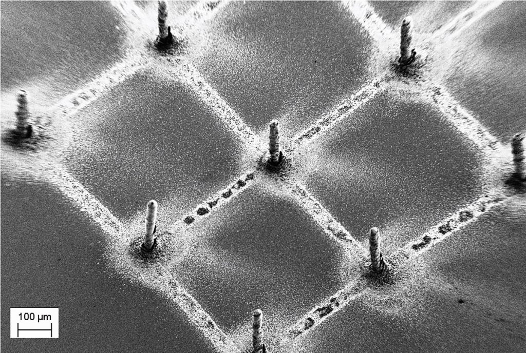
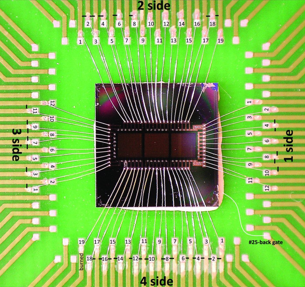
László and his team have discovered that to achieve this extraordinary sensitivity to X-rays, perovskite needs to be deposited in a very thin layer of carbon material called graphene, which strongly amplifies the signal generated by the X-rays. A further improvement for having highly detailed images with low doses of X-rays is to print this perovskite onto graphene in the form of pillars (imagine a bed of nails), using a method called 3D aerosol jet printing. This is a radically new approach, and where going down to the nanoscale is useful, as this method allows the layer to be printed with μm (micrometre) precision.
The new perovskite photodetector is also cheaper and faster to produce. The conventional approach involves a cumbersome and time-consuming method to grow a large silicon crystal, amorphous selenium or very expensive cadmium telluride, all of which need to be conducted with complex procedures – for example, silicon at high temperatures and under vacuum conditions.
In contrast, 3D aerosol jet printing is quick and easy. Perovskite is simply mixed with ink, but not standard liquid ink used in pens. In this case, the ink is a liquid that can dissolve perovskite and evaporate it almost immediately, keeping the material in place with incredible accuracy. “Using a rapid and cheap printing technique, we have structured and tested an X-ray detector unit, which shows a record sensitivity four orders of magnitude higher than the up-to-date perovskite devices,” says László.
Given the promising results so far, László and the team are looking for investors to continue developing and testing their prototype. They are very confident that this new X-ray detector could be a potential game changer for medical imaging. Not only is it cheaper to produce, but more importantly, it needs lower radiation levels, resulting in safer imaging systems.
As nanoscale science and technology become more embedded in our lives, new opportunities for a career in this field arise daily. There are many different sectors which would welcome a nanoscale scientist, including aerospace, medicine, forensics, the military and biotechnology. Nanoscience and nanotechnology are in high demand and offer good prospects for the future. According to Salary Expert, the estimated salary for a nanotechnology engineer will increase 8% over the next five years.
If you want to find out more, the École Polytechnique Fédérale de Lausanne offers regular outreach programmes. At one of these events, László’s laboratory demonstrated a nanomanipulator hooked to a joystick like the ones used in computer games. With this special device, students could feel the force needed to push an atom on a surface, or the force needed to cut a carbon nanotube. “The kids were amazed by the experience. I am sure that many of them will want to study with us”, enthuses László.
 PROFESSOR LÁSZLÓ FORRÓ
Laboratory of Physics of Complex Matter, École Polytechnique, Fédérale de Lausanne, Switzerland
FIELD OF RESEARCH: Physics, Nanoscale Science and Novel Electronic Materials
RESEARCH PROJECT: Developing a 3D aerosol- jet-printed perovskite X-ray photodetector.
FUNDER: ERC Advanced Grant and ERC Proof of Concept
ABOUT NANOSCALE SCIENCE
WHAT IS SO SPECIAL ABOUT NANOSCALE SCIENCE?
Nanoscale science – or nanoscience – is the study of materials on a truly small scale. This field of science may be relatively new, but it has a huge potential to change our world. From developing new materials, to energy related topics (photovoltaics, fuel cells, thermoelectrics), environmental challenges (water purification, protective and sterilising air filters), to breakthroughs in medicine (vectors for drug delivery, contrast agents in MRI, cancer treatment), the possibilities are endless. Such achievements are only possible with a cross-disciplinary approach, where scientists from a wide range of fields come together. All around the world, chemists, physicists, biologists, medical doctors, computer engineers and many others are studying nanoscience and using it to better understand and change our world.
JUST HOW SMALL IS NANOSCALE?
Nanoscale is the scale used to measure atoms and molecules, which means it is really tiny. You would need 10 hydrogen atoms stacked up on top of each other to reach 1 nanometre height, and a strand of DNA is only about 2.5 nanometres in diameter. If you imagine that everybody on Earth was only one nanometre tall, you could fit the entire population in a matchbox! That is how small nanoscale really is. Think small, then think smaller.
HOW CAN NANOSCIENCE CHANGE OUR VIEWS OF THE WORLD?
Thinking about how small we can go is fun, but the real value of nanoscale science is how chemical and physical properties of different materials change in the nanoworld. For example, we all know that gold is yellow, but break it down into nanosize nuggets and it can be orange, purple or green depending on the size and shape of each piece.
Reference
https://doi.org/10.33424/FUTURUM124


CT SCAN (OR COMPUTED TOMOGRAPHY SCAN) – involves multiple x-ray measurements taken from different angles to generate a tomographic image of the body
MICRO – a prefix meaning one millionth (1/1,000,000)
MICROMETRE (μM) – a distance unit representing one-millionth of a metre or one-thousandth of a millimetre. Also known as micron
NANO – a prefix meaning one billionth (1/1,000,000,000)
NANOMANIPULATOR – a device for controlling and manipulating individual molecules or nanoscale objects, such as an atomic force microscope
NANOMETRE (NM) – a distance unit representing one-billionth of a metre or one-millionth of a millimetre
NANOSCIENCE – science conducted at the nanoscale, which is between 1 and 100 nanometres
SURFACE AREA – a measure of the total area that the surface of the object occupies
X-RAY (X-RADIATION) – a type of radiation, known as electromagnetic waves, which is very energetic and can penetrate skin and internal organs
X-RAY PHOTODETECTOR (OR SIMPLY DETECTORS) – devices that can measure X-ray radiation. In a medical setting, these machines are usually imaging detectors. For many years, doctors used photographic plates and x-ray film, but now most have been replaced by computerised devices like flat panel detectors
X-rays are an essential medical imaging tool used by doctors all around the world. However, despite the obvious benefits for patients, this procedure is also associated with an increased risk of cancer. Professor László Forró, Head of the Laboratory of Physics of Complex Matter based at the École Polythechnique Fédérale de Lausanne, in Switzerland, wants to use the latest technology to develop a new device that requires significantly lower levels of radiation for the same image quality and, therefore, reduces health risks.
We may not think about it, but the simple act of getting an X-ray or a CT scan in a hospital or at the dentist’s surgery has the potential to be risky for our health. You cannot see them or feel them, but X-rays are like beams of invisible light with the ability to pass through your body. As they do this, the energy from these beams is absorbed differently in different tissues. An X-ray photodetector picks up the remaining X-rays on the other side of the body and creates a black and white image. Soft parts, like the heart and lungs, appear darker as the X-rays cross easily, whereas dense parts, like bone, appear white because the X-rays find it harder to cross.
This makes X-rays incredibly powerful tools to spot many diseases, like cancers, cardiovascular diseases and osteoporosis. The problem is that the radiation crossing our body can cause small changes in our DNA, which may produce mutations and cause cancer later in life.
HOW CAN WE LIMIT RADIATION EXPOSURE?
“The current imaging technique needs lots of very complex electronics. Making it simpler, easier and more user-friendly would be an advantage”, says László.
With this in mind, László’s team has been working on a new method to produce X-ray images using a significantly lower amount of radiation, all thanks to an inspiring new material: lead halide perovskites.
In the name of this synthetic material, ‘perovskite’ denotes the structure, which was first identified by Lev Perovski for a mineral originally discovered in Russia. Typically, this compound includes several chemical elements with both positive and negative charges, such as lead, bromine or iodine, arranged in a complex octahedron.
Researchers have known about the curious properties of these perovskites at the nanoscale for a while, but only recently started using it in different devices, including lasers, light-emitting diodes, gas sensors and photodetectors. Most of these are still in the development stage in the lab, but have perovskite-based solar panels – the first product to be created – are already on their way to commercialisation either as a standalone product or in combination with other types of solar panels.
Forging a new use for this material, László developed the element of an X-ray photodetector with a thin layer of perovskite, which turned out to be several times more sensitive than conventional detectors. It is still in its early stages, but this new device seems to be able to catch more X-rays – which would be lost in conventional detectors – due to the presence of heavy elements such as lead and iodine in perovskite. As a result, László’s perovskite-based detector easily outperforms silicon-based traditional X-ray detectors.
The researchers believe this high sensitivity will allow medical and dental images to be obtained with only a fraction of the radiation compared to normal X-ray imaging. This is good news as lower levels of exposure reduce the risk of cancer for both patients and health care professionals. Other uses, which may also benefit from a more efficient X-ray detector, include revealing counterfeit art and scanning luggage in airports.
HOW IS PEROVSKITE PRINTED?
László and his team have discovered that to achieve this extraordinary sensitivity to X-rays, perovskite needs to be deposited in a very thin layer of carbon material called graphene, which strongly amplifies the signal generated by the X-rays. A further improvement for having highly detailed images with low doses of X-rays is to print this perovskite onto graphene in the form of pillars (imagine a bed of nails), using a method called 3D aerosol jet printing. This is a radically new approach, and where going down to the nanoscale is useful, as this method allows the layer to be printed with μm (micrometre) precision.
The new perovskite photodetector is also cheaper and faster to produce. The conventional approach involves a cumbersome and time-consuming method to grow a large silicon crystal, amorphous selenium or very expensive cadmium telluride, all of which need to be conducted with complex procedures – for example, silicon at high temperatures and under vacuum conditions.
In contrast, 3D aerosol jet printing is quick and easy. Perovskite is simply mixed with ink, but not standard liquid ink used in pens. In this case, the ink is a liquid that can dissolve perovskite and evaporate it almost immediately, keeping the material in place with incredible accuracy. “Using a rapid and cheap printing technique, we have structured and tested an X-ray detector unit, which shows a record sensitivity four orders of magnitude higher than the up-to-date perovskite devices,” says László.
Given the promising results so far, László and the team are looking for investors to continue developing and testing their prototype. They are very confident that this new X-ray detector could be a potential game changer for medical imaging. Not only is it cheaper to produce, but more importantly, it needs lower radiation levels, resulting in safer imaging systems.
As nanoscale science and technology become more embedded in our lives, new opportunities for a career in this field arise daily. There are many different sectors which would welcome a nanoscale scientist, including aerospace, medicine, forensics, the military and biotechnology. Nanoscience and nanotechnology are in high demand and offer good prospects for the future. According to Salary Expert, the estimated salary for a nanotechnology engineer will increase 8% over the next five years.
If you want to find out more, the École Polytechnique Fédérale de Lausanne offers regular outreach programmes. At one of these events, László’s laboratory demonstrated a nanomanipulator hooked to a joystick like the ones used in computer games. With this special device, students could feel the force needed to push an atom on a surface, or the force needed to cut a carbon nanotube. “The kids were amazed by the experience. I am sure that many of them will want to study with us”, enthuses László.
DR LÁSZLÓ FORRÓ
Laboratory of Physics of Complex Matter, Ecole Polytechnique, Fédérale de Lausanne, Switzerland
FIELD OF RESEARCH: Physics, Nanoscale Science and Novel Electronic Materials
RESEARCH PROJECT: Developing an 3D aerosol- jet-printed perovskite X-ray photodetector.
FUNDER: ERC Advanced Grant and ERC Proof of Concept
ABOUT NANOSCALE SCIENCE
WHAT IS SO SPECIAL ABOUT NANOSCALE SCIENCE?
Nanoscale science – or nanoscience – is the study of materials on a truly small scale. This field of science may be relatively new, but it has a huge potential to change our world. From developing new materials, to energy related topics (photovoltaics, fuel cells, thermoelectrics), environmental challenges (water purification, protective and sterilising air filters), to breakthroughs in medicine (vectors for drug delivery, contrast agents in MRI, cancer treatment), the possibilities are endless. Such achievements are only possible with a cross-disciplinary approach, where scientists from a wide range of fields come together. All around the world, chemists, physicists, biologists, medical doctors, computer engineers and many others are studying nanoscience and using it to better understand and change our world.
JUST HOW SMALL IS NANOSCALE?
Nanoscale is the scale used to measure atoms and molecules, which means it is really tiny. You would need 10 hydrogen atoms stacked up on top of each other to reach 1 nanometre height, and a strand of DNA is only about 2.5 nanometres in diameter. If you imagine that everybody on Earth was only one nanometre tall, you could fit the entire population in a matchbox! That is how small nanoscale really is. Think small, then think smaller.
HOW CAN NANOSCIENCE CHANGE OUR VIEWS OF THE WORLD?
Thinking about how small we can go is fun, but the real value of nanoscale science is how chemical and physical properties of different materials change in the nanoworld. For example, we all know that gold is yellow, but break it down into nanosize nuggets and it can be orange, purple or green depending on the size and shape of each piece.
Scientists have learnt how to change properties such as colour, conductivity or even strength by controlling how these nanosize particles are formed. This is incredible, because they are not changing the chemical composition, they are changing the size of each particle. This happens because as more of the material’s surface area is exposed, these tiny particles become incredibly reactive. This phenomenon opens so many doors to improve virtually all manufacturing processes and make them more energy efficient. The 3D aerosol-jet-printed perovskite X-ray photodetector is just one example of this.
ARE NANOSCIENCE AND NANOTECHNOLOGY THE SAME THING?
These two terms are often used interchangeably. They are not exactly the same thing but are interlinked. Nanoscience is the study of the very small, whereas nanotechnology involves building devices and structures at the nanoscale. Essentially, nanoscience studies materials and their properties at the nanoscale and then nanotechnology uses them to create something new.
HOW TO BECOME A NANOSCALE SCIENTIST
• This is an incredibly varied field. For some positions, you may need experience working in a laboratory environment, while others may prefer a background in industry.
• Nanowerk in Europe and Nano4me in the USA are good starting points to look for positions in nanotechnology and nanoscience.
• According to Salary Expert, an experienced nanoscientist or nanotechnologist may earn up to CHF 91’811 (about £76K) per year.
PATHWAY FROM SCHOOL TO NANOSCIENCE AND NANOTECHNOLOGY
• To start a career in nanoscale science, you need a degree in one or more of the fundamental sciences, such as physics, chemistry or even biology. Other relevant courses include electronics, engineering and materials science.
• Most colleges and universities offer specialised courses in nanoscience and nanotechnology.
• Postgrad.com lists establishments that offer postgraduate courses in nanotechnology.
• If you are interested in finding out more about the nano world, the National Nanotechnology Initiative in the US offers a wide range of educational resources from secondary school to postgrad level.
HOW DID LÁSZLÓ BECOME A NANOSCALE SCIENTIST?
WHAT WERE YOUR INTERESTS AS A CHILD?
Many! I used to read a lot, but I was also fond of art and natural sciences. Although I grew up in a modest family, I had many positive influences in my environment. I received all the support I needed from my parents to study.
WHO OR WHAT INSPIRED YOU TO BECOME A SCIENTIST?
In secondary school, I regularly attended competitions in maths and physics, and met interesting people, who became friends and forged my interest and motivation in science. And, of course, reading the biographies of scientists helped me a lot.
WHAT ATTRIBUTES HAVE MADE YOU A SUCCESSFUL SCIENTIST?
Imagination and creativity are essential for being a successful scientist. But the prerequisite is very good technical knowledge, so university studies are very important. In physics, what we learn, what we are trained for, is problem solving. We have analytical minds. This is very important.
HOW DO YOU OVERCOME OBSTACLES IN YOUR WORK?
We can have many kinds of problems: human, technical, conceptual. The most difficult ones are human obstacles. But with a positive attitude, you can solve most of them.
WHAT ARE YOUR PROUDEST CAREER ACHIEVEMENTS?
I have several achievements, which start with the sentence, “for the first time, we have managed to…”.
I can give you one example: Cells maintain their form with the help of protein polymers called microtubules. These are also the ‘wires’ which pull apart the chromosomes during cell division. Their diameter is only 24 nanometres; one cannot see them. Nobody has measured how mechanically strong they are, but it is an important quantity to describe how the cell functions. One of my post-docs managed to extract just a few grams of these microtubules from a cow’s brain and elaborated a method to measure its mechanical strength. Since then, many scientists have applied our method to measure nanoscale biological structures. I can say that I am proud of this path to discovery, because it needed imagination and conviction to do it.
LÁSZLÓ’S’ TOP TIPS
01 Take your science subjects seriously!
02 Do not be afraid to dream, to have a vivid imagination, and to have the courage to go to unexplored fields.
03 It is important to read, to be fond of art, to be a colourful person. Beyond the fact that it is a great intellectual pleasure to enjoy art, it will help you to develop your imagination and communication skills.
04 Forging a network of supportive people, including colleagues and friends, is also very important to be successful.
Write it in the comments box below and László will get back to you. (Remember, researchers are very busy people, so you may have to wait a few days.)